
8051 Development System Circuit Board 3
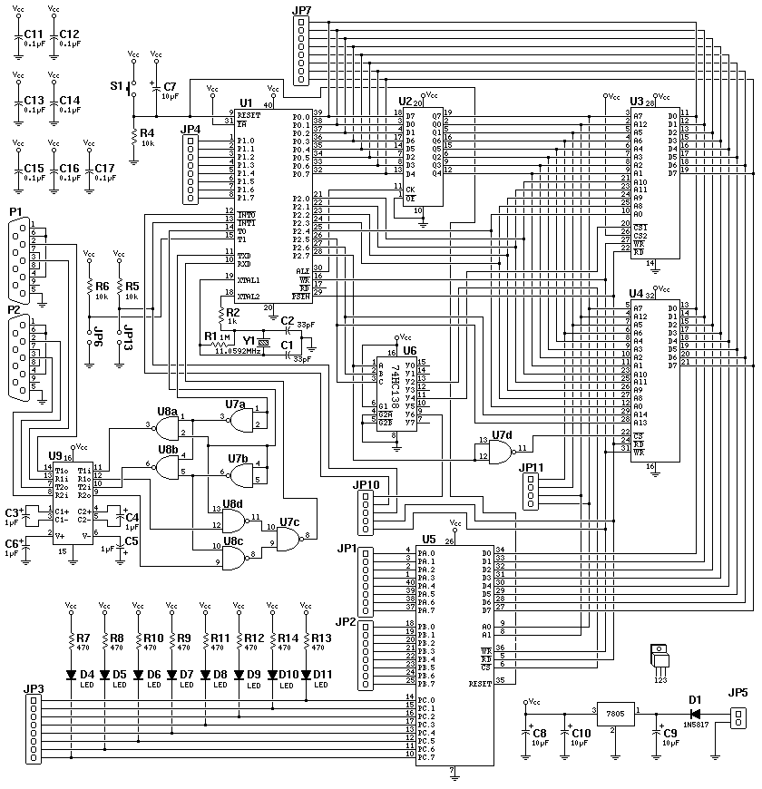
The circuit board described is a sophisticated development platform that incorporates various modern enhancements over its predecessor. The Rev 4 version features a faster CPU, expanded memory capabilities, and increased input/output options, including an optional LCD interface. This makes it particularly suitable for contemporary projects requiring enhanced performance and flexibility.
The schematic is designed with separate address and data bus connections, which simplifies manual wiring if desired. This approach provides clarity during assembly, especially for those engaging in hand-wiring techniques, such as wire-wrapping or point-to-point soldering. The design minimizes wire crossings, contributing to a cleaner layout and easier troubleshooting.
The address bus wiring utilizes an unconventional scheme that facilitates efficient point-to-point connections. This design choice allows for a simplified PCB layout, accommodating wider traces and fewer vias, which is advantageous for signal integrity and overall performance. The use of the 74HC373 flip-flop chip standardizes the data line connections, ensuring that any flip-flop can be utilized interchangeably without affecting functionality.
Data storage and retrieval are managed by the 87C52 microcontroller, which writes to both RAM and Flash ROM. The architecture allows for flexibility in the physical mapping of memory locations, as the read operations will consistently return the data previously written, regardless of the specific address used.
The MAX232 chip serves as a crucial component for serial communication, facilitating RS-232 connections. The choice of capacitor values, while flexible, can influence performance characteristics, particularly in relation to noise filtering and charge-pump operation. The memory map provided outlines the various address ranges allocated for different functionalities, including monitor access, SRAM, I/O operations, expansion capabilities, and Flash ROM.
Overall, the circuit board represents a well-thought-out design that balances modern requirements with practical assembly considerations, making it a valuable resource for developers and engineers working on embedded systems and related applications.A newer version of this circuit board is available. Rev 4 includes a faster CPU, more memory, more I/O and an optional LCD. We recommend you use Rev 4 for new projects. Even though this older board is no longer available, we are keeping these old pages on-line for reference to assist people who purchased or build the older version. This i s the complete schematic for the development board. Address and Data bus wires are drawn separately (not in a bus), so that it`s easy to color over them on a printout, if you choose to manually connect the wires. It really is easier to buy a bare circuit board, though. This design and its schematic have been placed in the public domain. They are distributed in the hope that they will be useful, but are provided without any warranty, not even a warranty of merchantability or fitness for a particular purpose.
The address bus in this schematic is connected in an unusual way, which is optimized for simpler point-to-point wiring. For anyone building the board using wire-wrap or hand soldered point to point construction, this wiring scheme makes for much less clutter in the wiring if the chips are positioned similarily to the layout on the printed circuit board.
Very few wires cross over one another. This also makes the PC board layout a bit simpler, allowing wider traces and fewer vias. This unusual address bus wiring works. The 74HC373 chip (U2) is 8 identical flip-flops, so it does not matter which one is used for each line. On the RAM (U3) and Flash ROM (U4) chips, all data that is stored in these chips is written by the 87C52 chip (U1), so it does not matter which physical location within the chip is mapped into each location within the CPU`s address space, because each read from these chips will return the same data that was written from a previous write.
Some readers have felt that it`s "just not natural" to connect any other way than P0. 0-D0-Q0-A0, P0. 1-D1-Q1-A1, and so on, but it does indeed work. For a historic example, Woz used a very creative address bus connection scheme in the Apple ][ to automatically do DRAM refresh with his video refresh reads. Because he arranged the address pins a certain unusual way, every video mode accessed each DRAM row several times per video refresh, so he didn`t need to add the cost and space of the usual DRAM refresh circuits (he interleaved video and cpu memory access, since the 6502 spends half its time not fetching anything).
It works, and Apple sold millions of them! The MAX232 chip (U9) is shown with C3, C4, C5, and C6 as 1 µF, but the board is usually built with 10 µF capacitors (as shown in the parts list below). Either will work. C6 is connected to ground. In the sample circuit within the datasheet, it is connected to Vcc. Either connection will work. This connection causes charge-pump current flow through C8 and C10, but it avoids coupling the Vcc line to the V+ pin (high frequency digital switching noise, relative to ground, despite C11-C17).
The V+ pin is ultimately connected via the MAX232 driver to the RS-232 cable. 0000 - 1FFF PAULMON2 Monitor 2000 - 3FFF SRAM 4000 - 5FFF 82C55 I/O Chip 4000: Port A (read or write) 4001: Port B (read or write) 4002: Port C (read or write) 4003: Configure (write only) 6000 - 7FFF User Expansion (Y6 signal assert low) 8000 - FFFF Flash ROM 🔗 External reference
Related Circuits
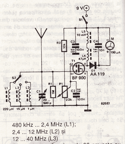
An RF field indicator is needed to verify power stages and transmitter antennas. This radio field indicator allows for the measurement of radiated energy from antennas. An RF field indicator is a crucial device in the field of telecommunications and...
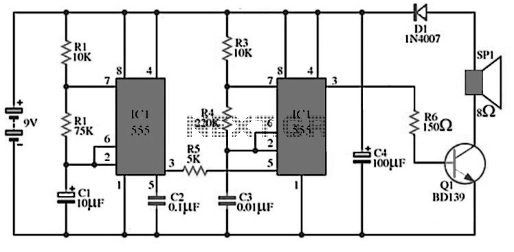
The circuit utilizes IC1 to create an astable multivibrator configuration. It is designed to generate a low-frequency output of approximately 1 Hz at pin 3, which is determined by the resistor values R1, R2 and capacitor C1. The output...
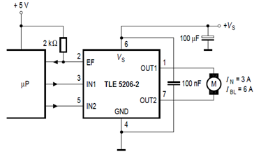
The schematic below illustrates the TLE5206-2 5A H-Bridge circuit for DC motor applications. This device features an integrated power H-bridge with DMOS output stages designed specifically for driving DC motors, as indicated in the datasheet. The TLE5206-2 circuit application...

The motorcycle anti-theft alarm circuit consists of several components, including the anti-theft detection circuit, the control circuit, the sound generator, the audio oscillator, and the power amplifier output circuit, as illustrated in figure 7-91. The anti-theft detection circuit is...
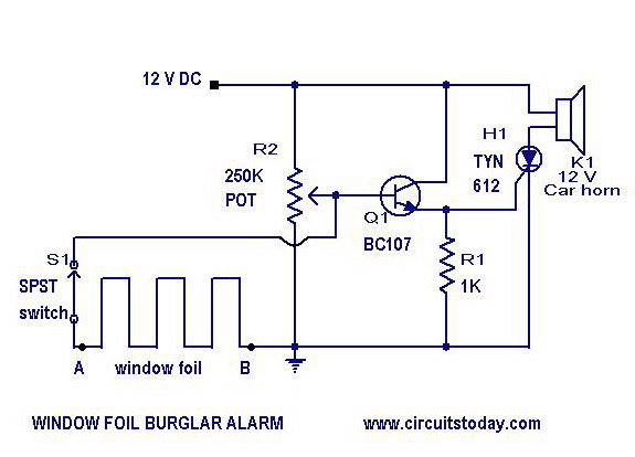
A simple burglar alarm circuit diagram and schematic. This can be used as an anti-theft alarm by attaching the burglar alarm circuit to window foil. The burglar alarm circuit is designed to provide a basic security solution for residential or...
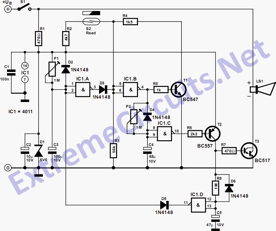
The circuit presented is a simple yet effective alarm system designed to protect an object. It requires no specialized devices and can be constructed using commonly available components. The primary alarm-triggering element is a reed switch. Any optical or...
Warning: include(partials/cookie-banner.php): Failed to open stream: Permission denied in /var/www/html/nextgr/view-circuit.php on line 713
Warning: include(): Failed opening 'partials/cookie-banner.php' for inclusion (include_path='.:/usr/share/php') in /var/www/html/nextgr/view-circuit.php on line 713