
830MHz RF2104 power amplifier schematic circuit configuration

The RF2104 amplifier circuit is designed for high-frequency applications, operating at 830MHz, making it suitable for various RF communication systems. The preamplifier stage is crucial for boosting weak RF signals before they reach the main amplification stage, ensuring that the subsequent amplification is effective and maintains signal integrity.
The output section of the circuit is carefully designed to provide an optimal impedance match between the amplifier and the load. The output matching network plays a vital role in maximizing power transfer and minimizing signal reflections, which could otherwise degrade performance. The choice of a 10nH shunt inductor aids in tuning the output stage to achieve the desired impedance characteristics.
The gain control feature via pin 8 allows for flexibility in the amplifier's performance, enabling users to adjust the amplification level based on the application requirements. This control can be particularly useful in environments where signal conditions fluctuate, allowing the amplifier to adapt and maintain optimal performance.
Overall, the RF2104 amplifier circuit exemplifies a well-engineered solution for enhancing RF signals, with features that cater to both performance and adaptability in various electronic applications. As shown in FIG constituted by RF2104 830MHz *** amplifier circuit works. Radio frequency (RF) signal from 5 feet input, via a preamplifier, amplified by an amplifier stage aft er the end of the 12-pin output. 5 feet with DC voltage, 5 feet plus a DC blocking capacitor coupling, while in parallel with a shunt inductor (10nH), 5 feet input impedance of 50. 12,13 pin output terminal is connected inside the chip, usually 13-14 feet connected together externally as a signal output, the output matching network connected, the amplifier output impedance to match the impedance of the load pin 5 + j0 when available obtain maximum output power.
13-14 feet is also connected with an external power supply as the end of the final stage amplifier. 8 feet to power control pin (PC), you can control the pin is connected to 0V and 3V gain, thereby controlling power; when the gain control is not required, the foot may be connected to a fixed voltage of 2.5 ~ 3V; the feet to the inflow of 2.5V voltage pin maximum current 1mA.
Related Circuits

This is an automatic light dimmer circuit that eliminates the need for manual adjustment of light levels. It utilizes a Light Dependent Resistor (LDR) to detect ambient light conditions, which in turn controls a Triac to adjust the brightness...
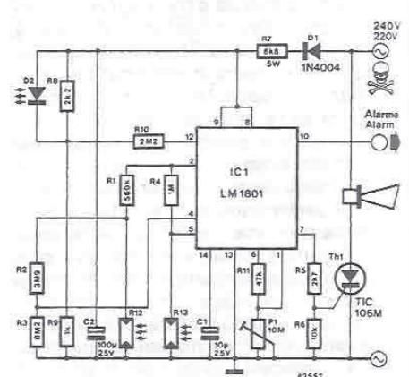
This smoke detector electronic project is designed using the LM1801 and common electronic components. The smoke detector circuit diagram does not utilize ionization detection, gas sensors, or optocouplers; instead, it employs two photoresistors (LDRs) and an LED. The circuit...
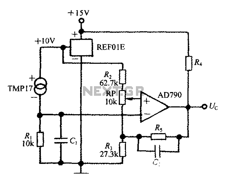
An adjustable thermostat controller circuit is widely used in everyday applications, such as for maintaining a constant temperature in soldering irons. The circuit utilizes the TMP17 sensor along with the REF01E voltage reference to ensure a stable 10V supply...
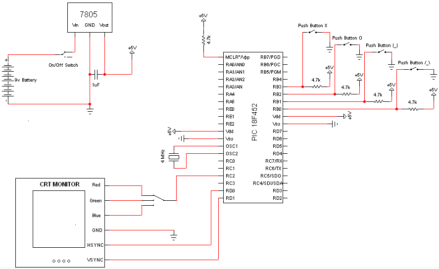
Very few electronic components are required for this project, as the PIC Microcontroller serves as the primary processing unit. The essential components include buttons, switches, and a power circuit, which are straightforward forms of input/output, facilitating an easier understanding...
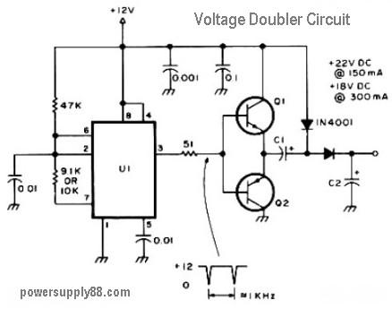
This circuit diagram represents a DC voltage doubler and DC converter. It is designed to convert a 12V DC power supply into outputs of 24V DC and 18V DC. Nearly any PNP or NPN power transistors can be utilized...
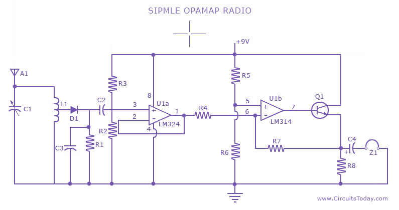
A low-cost, simple radio circuit schematic using an operational amplifier. This radio circuit diagram consists of a sensitive audio amplifier that receives strong signals. The presented radio circuit schematic utilizes an operational amplifier (op-amp) to create a cost-effective and straightforward...