
880MHz low-noise amplifier application circuit composed of RF2347

The RF2347 low noise amplifier circuit operates effectively at a frequency of 880 MHz, making it suitable for various RF applications. The design incorporates a direct coupling mechanism from the input pin (pin 3) to the amplifier, allowing for minimal signal degradation. The use of a 22 pF blocking capacitor ensures that DC components do not interfere with the RF signal, thereby preserving the integrity of the amplified output.
The output stage, located at pin 7, is configured as an open collector, enabling flexibility in connecting to different power supply configurations through a choke or matching inductor. This design choice allows for efficient impedance matching, which is critical for maximizing output power and overall circuit efficiency. The external output matching network is crucial in aligning the amplifier's output impedance to the standard 50 ohms, facilitating optimal power transfer to subsequent stages or antennas.
Pin 1 serves a dual purpose as the power down control terminal, providing a means to manage the biasing of the amplifier. The circuit is designed to operate at a nominal voltage of 2.8 V, drawing a typical current of 8.5 mA, which indicates the active state of the amplifier. Conversely, when the voltage at VPD drops to 0.9 V, the amplifier enters a low-power state, effectively shutting down to conserve energy. An additional RF bypass circuit is recommended to stabilize the operation of the amplifier during transitions between active and inactive states, ensuring reliable performance across varying conditions. Overall, this low noise amplifier design is well-suited for applications requiring high gain and low noise performance in the RF spectrum. As shown in FIG constituted by 880MHz RF2347 low noise amplifier application circuit. Radio frequency (RF) signal from the input pin 3, after the output of the amplifier 7 feet . 3 feet and the internal amplifier is directly coupled, so 3 feet plus a 22pF blocking coupling capacitance, impedance matching at 836MHz work as 50. 7 feet for the open collector output terminal can be connected to the power supply Vcc through choke or matching inductor, the pin impedance matching is typically 50, external output matching network allows the amplifier output impedance matching for maximum output power and efficiency.
1 foot for the power down control terminal for controlling bias. When VPD (2.8 0.1) V when (IPD is typically 8.5mA) circuit; when VPD 0.9V circuit closes; VPD requested additional RF bypass circuit.
Related Circuits

This circuit is designed for differential analog circuit switches. The FM1208 monolithic dual differential multiplexer is utilized in applications where the RDS (ON) must be closely matched. The RDS (ON) for the monolithic dual multiplexer operates with a precision...
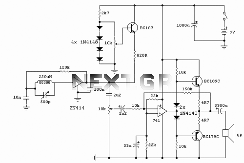
This receiver, designed around the popular ZN414 integrated circuit, operates within the AM band frequency range of 550 to 1600 KHz. For Longwave reception, it is necessary to replace the coil, which can be sourced from an old medium...
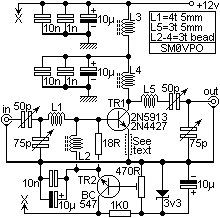
Once again my collection of projects creation has been interrupted by another necessity. Patrick and other people have asked me for a circuit of a VHF power amplifier. These circuits are my "standard" building blocks that can be used...
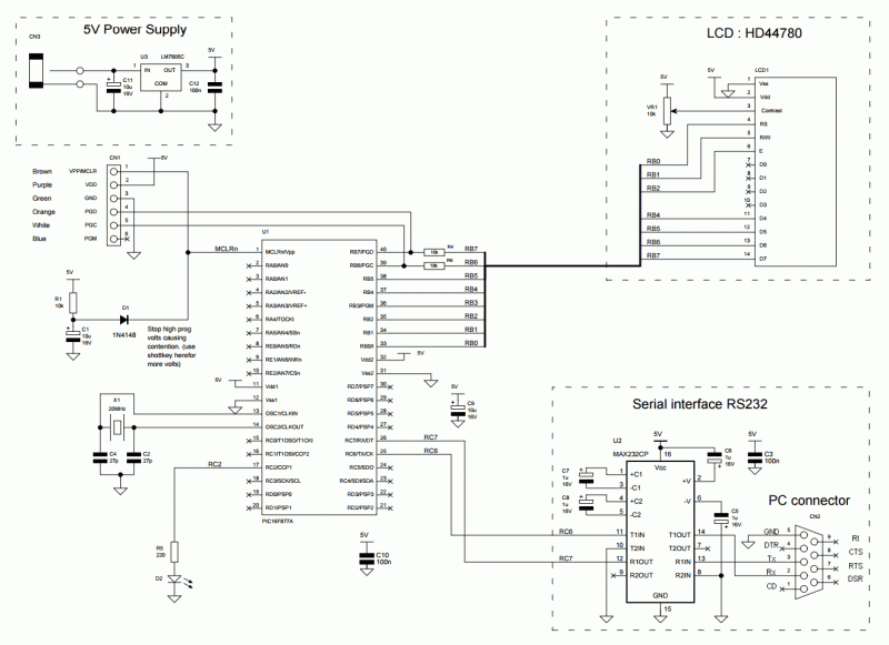
The circuit consists of a PIC microcontroller, an in-circuit serial programming (ICSP) interface, an RS232 level translator, and an HD44780 LCD display. Initially, a scrolling message is shown using the show_intro function. When a serial input is detected, the...
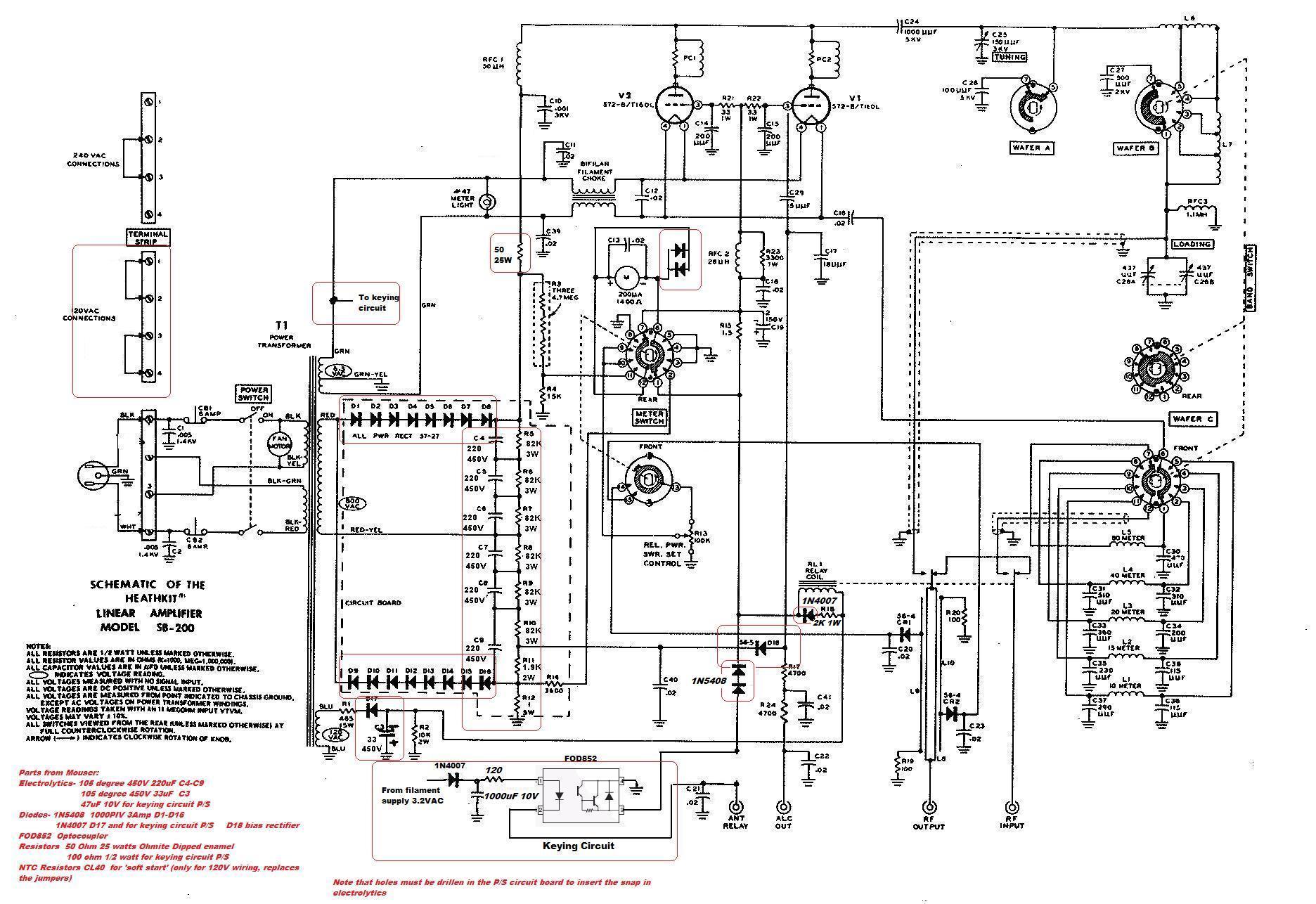
This circuit serves as a cost-effective alternative to commercially available keying circuits. It has been successfully implemented in the SB-200 amplifier. A schematic of the modified SB-200 is provided. The described circuit is designed to function as a keying mechanism...
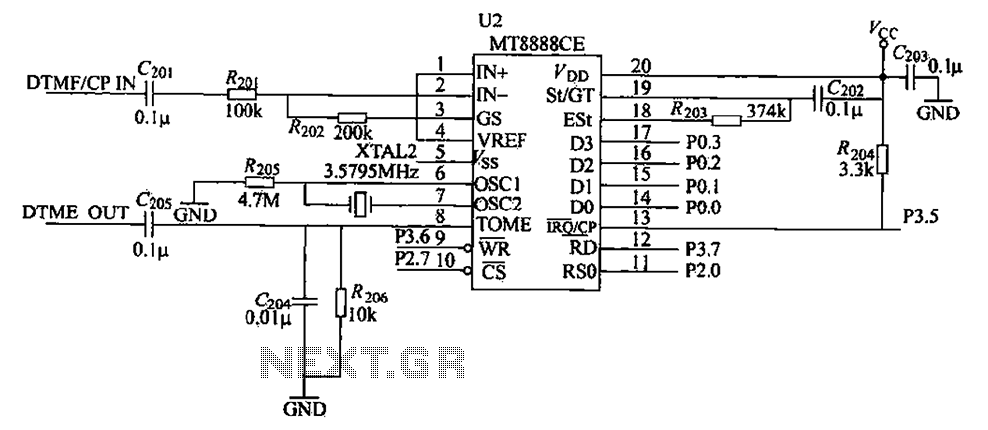
The automatic alarm circuit comprises a DTMF automatic dialing system, a password control circuit, a voice detection and alarm circuit, a telephone interface circuit, a power supply circuit, and a keyboard display circuit. The automatic dial-up alarm utilizes the...