
Heath SB-200 keying circuit

The described circuit is designed to function as a keying mechanism for RF amplifiers, specifically tailored for the SB-200 model. The keying circuit allows for the controlled operation of the amplifier, ensuring that it engages and disengages efficiently during transmission and reception modes.
The schematic typically includes essential components such as transistors, resistors, capacitors, and diodes, which work together to create a reliable switching mechanism. The transistors are often used as switches to control the flow of power to the amplifier, while resistors and capacitors help to manage the timing and stability of the circuit.
In a standard configuration, a small signal from a transmitter or keying device is fed into the base of a transistor, which then allows a larger current to flow from the power supply to the amplifier, effectively turning it on. Conversely, when the signal is removed, the transistor cuts off the current, turning off the amplifier. This method not only provides an economical solution but also ensures that the amplifier operates safely and effectively without the need for expensive commercial keying circuits.
In summary, this modified keying circuit is a practical and efficient solution for users seeking to enhance their SB-200 amplifier's performance while minimizing costs. The schematic serves as a valuable reference for those looking to implement similar modifications in their equipment.For those who may want to try a cheaper alternative to the commercially available keying circuits. Works well in my SB-200. Here is a schematic of my modified SB-200.. 🔗 External reference
Related Circuits
The circuit generates a controlled pulse signal. When a high pulse signal is applied to the input terminal O (start), the output pulse signal is activated. Conversely, when a low signal is received at the input terminal O (stop),...

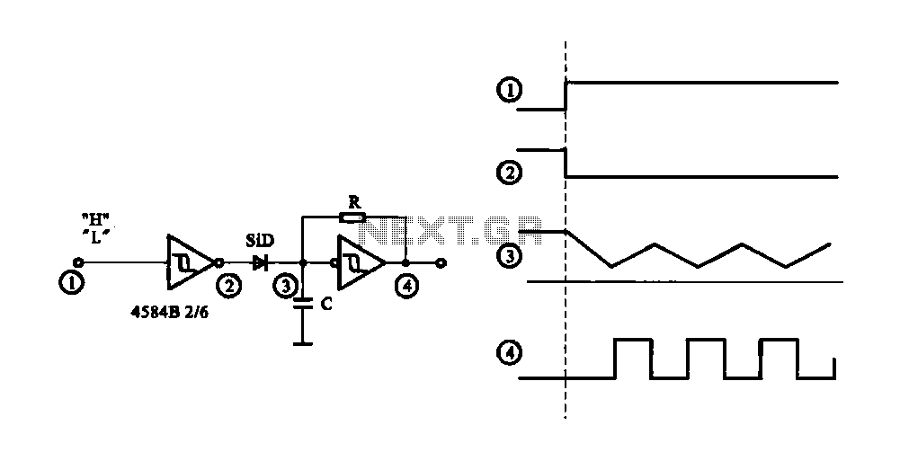
The circuit operates as an astable multivibrator, generating a square wave signal at a specific frequency. When powered, the circuit will function continuously. The astable multivibrator circuit is a type of oscillator that produces a continuous square wave output without...

A tone generator circuit, which can be used to create a simple calling bell circuit, is illustrated here. It is constructed using the 8021 integrated circuit (IC), which includes built-in circuitry for producing a "ding-dong" sound. The tone generator circuit...
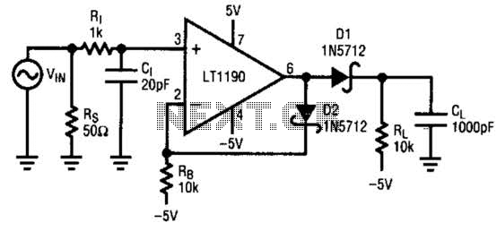
A fast pulse detector can be constructed using this circuit. A very fast input pulse will surpass the amplifier's slew rate, resulting in a prolonged overload recovery time. Implementing some degree of dv/dt limiting on the input can alleviate...

The static display circuit is illustrated in Figure 6. The 74LS244 acts as bus drivers, and six figures represent a public bus, each equipped with an LED display latch (like the 74LS273) connected to the code for latching the...

This circuit is a simple analog multiplier. The operation of the circuit can be understood by considering A2 as a controlled gain amplifier. It involves components such as an analog multiplier, a log-antilog circuit, and a summing junction, along...