
A circuit diagram of the digital pressure signal conditioner MAX1459 4 ~ 20mA current transmitter
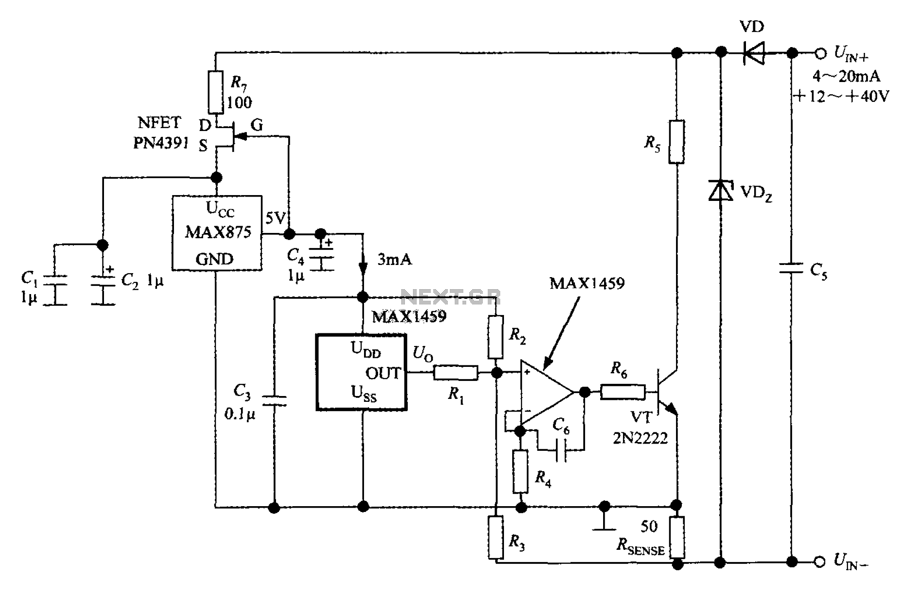
The 4 to 20 mA current transmitter circuit is designed for robust performance in industrial applications, where precise current signaling is critical. The choice of the MAX1459 as the core component allows for effective signal processing, enabling accurate temperature and gain compensation, which is essential for maintaining signal integrity across varying environmental conditions. The integration of the PN4391 NFET and the MAX875 bandgap reference ensures that the circuit can deliver a stable and reliable current output, even in the presence of varying load conditions and cable resistances.
The output stage of the circuit, which includes the spare amplifier and the external power amplifier, is pivotal in achieving the desired current output. This configuration allows for flexibility in the loop supply voltage, accommodating a range from +12V to +40V, making the circuit suitable for various applications. The use of the 2N2222 power transistor provides sufficient drive capability, ensuring that the circuit can handle the required current levels without overheating or failing.
The calibration process, involving the adjustment of RSENSE and the associated resistors R1 to R4, is crucial for achieving the desired output characteristics. The ability to calibrate the output voltage across RSENSE to a standard range of 0.2 to 1.0V allows for easy integration into existing systems and enhances the versatility of the transmitter.
Decoupling and filtering capacitors (C1 to C5) are strategically placed to minimize noise and ensure stable operation of the circuit, while the frequency compensation capacitor (C6) helps maintain the stability of the amplifier stages. The careful selection of component values and types throughout the circuit contributes to the overall performance, reliability, and accuracy of the 4 to 20 mA current transmitter, making it a valuable solution for industrial measurement and control applications.4 ~ 20mA current transmitter circuit from the MAX1459 configured as shown in FIG. The PGA output voltage supplied to the spare amplifier chip, and then through an external powe r amplifier can obtain 4 ~ 20mA current output, the current long-distance transmission, the accuracy of the current signal is not affected by cable resistance. PN4391 to 40V, 150mA N-channel FET (NFET). MAX875 low-power, low drift 5V bandgap reference voltage source, the voltage temperature coefficient of 7 10-6/.
Constituted by the PN4391 and MAX875 3mA of constant current source, to provide a stable operating current MAX1459, MAX1459 re-use temperature compensation and gain compensation (not shown pressure sensor). MAX1459 output voltage sequentially through spare amplifier, power amplifier into a current signal 4 ~ 20mA, allowing loop supply range is + 12 ~ 40V.
VT use 2N2222 type power tube, its main parameters: UCEO 60V, ICM 0.8A. In UIN +, UIN- a parallel between the regulator, overvoltage protection can play a role. The initial voltage across the sense resistor RSENSE set by resistors R1 ~ R4, the signal voltage across RSENSE is controlled by the MAX1459. When RSENSE 50, the available standard voltage 0.2 ~ 1.0V calibrated. C1 ~ C3 as a decoupling capacitor, C4, C5 for the filter capacitor, C6 frequency compensation capacitor.
R5, R6, respectively collector resistance and base resistance.
Related Circuits
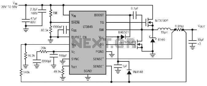
Burst Mode operation maintains high efficiency at light loads by reducing IC quiescent current to 120 µA. Light load efficiency is also improved with the reverse inductor current inhibit function, which supports discontinuous operation. Additional features include an adjustable...
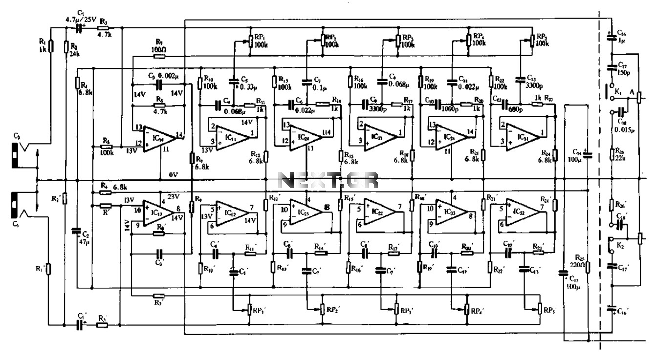
Figure 1-98 illustrates a double five-band equalizer circuit featuring a secondary connection. In this configuration, IC1 and IC14 serve as voltage amplifiers for each channel of the equalizer. The circuit also includes IC11, IC24, IC2, IC34, IC31, IC12, IC23,...
Many amateur receivers are equipped with an S meter that does not operate logarithmically. The proposed circuit is intended to enhance such receivers. Although integrated circuits like the CA3089 or CA3189 are not commonly used today, they play a...
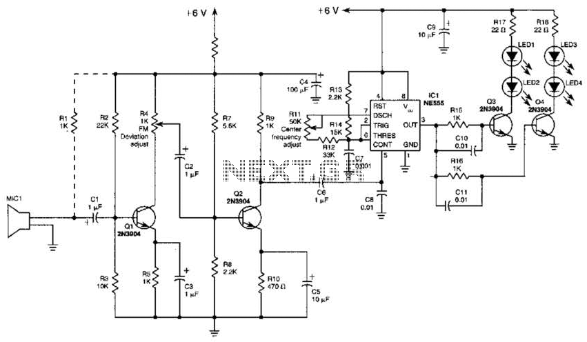
This transmitter employs a two-stage amplifier configuration using transistors Q1 and Q2 to frequency modulate an NE555 timer, which is set up as a voltage-controlled oscillator (VCO) operating at approximately 50 kHz. The resulting frequency-modulated pulse train is transformed...
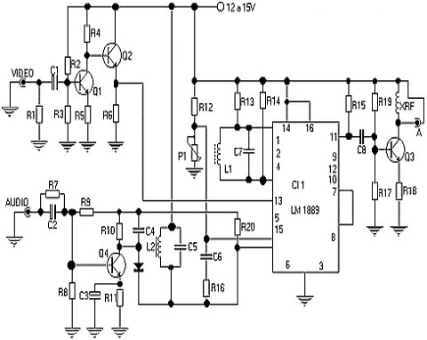
The following circuit illustrates a simple TV transmitter circuit diagram. This circuit is based on the LM1889 integrated circuit (IC). Features include quadrature chroma modulators and RF capabilities. The circuit utilizes the LM1889 IC, which is designed for television applications,...
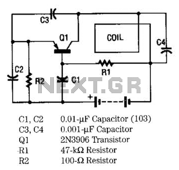
The metal locator utilizes a one-transistor oscillator in conjunction with an AM radio to detect metal. Transistor Q1 is a PNP transistor connected to the oscillator circuit. Resistor R1 supplies the appropriate base bias, while capacitors C3 and C4,...
Warning: include(partials/cookie-banner.php): Failed to open stream: Permission denied in /var/www/html/nextgr/view-circuit.php on line 713
Warning: include(): Failed opening 'partials/cookie-banner.php' for inclusion (include_path='.:/usr/share/php') in /var/www/html/nextgr/view-circuit.php on line 713