
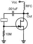
A Low-Frequency Crystal Controlled Oscillator

The circuit design features a low-frequency sine wave oscillator that is particularly effective for testing quartz crystals in the specified frequency range. The use of AF bipolar transistors in the oscillator and amplifier stages ensures cost-effectiveness and reliability. The modified astable multivibrator configuration, with automatic loop gain adjustment, allows for stable oscillation even in the presence of component variations and environmental factors.
The incorporation of a JFET for loop-gain control is a critical aspect of the design, as it allows for real-time adjustments to the oscillator's performance, maintaining output stability. The careful selection of components, including the Zener diode and resistors, enhances the circuit's resilience to power supply variations, which is particularly important in laboratory settings where precision is paramount.
The detailed specifications regarding the capacitor values and resistor configurations provide essential guidance for engineers seeking to optimize the circuit for specific crystal characteristics. The inclusion of a BNC connector and a three-way switch for frequency selection further enhances the versatility of the instrument, making it suitable for a wide range of testing applications.
Overall, this circuit represents a robust solution for RF engineers requiring a reliable method to test low-frequency quartz crystal units, addressing common challenges associated with existing equipment and providing a practical alternative for laboratory use.The RF engineer sometimes has to look for an instrument that will check a low frequency quartz crystal unit reliably and rapidly. This is a difficult piece of equipment to find and the engineer often has to consult an electronic circuits handbook for the schematic of a circuit that will perform the task.
Unfortunately, there aren`t many such circu its in the technical literature currently available, and when found, they don`t always work as expected. A circuit that has been found to work at full satisfaction in the frequency range from 10 kHz to 500 kHz is illustrated in Figure 1.
This is a schematic of a low frequency sine wave oscillator featuring low distortion, wide-band operation and crystal control. The circuit, originally developed for laboratory use, employs low cost AF bipolar transistors for the oscillator and amplifier sections and a JFET for loop-gain control.
Operation of the oscillator in the 10 kHz to 500 kHz frequency range has been found to be excellent, while measured distortion is kept under 0. 1 percent Q1, Q2 and associated circuitry form a modified astable multivibrator in which the loop gain is automatically adjusted to the threshold of oscillation by means of field effect transistor Q3.
Q4 linearly amplifies the signal present at the collector of Q2 and isolates the oscillator section of the circuit from the output. This stage features wide-band operation and delivers a clean 2. 5 Volt amplitude sine wave into a resistive load greater than or equal to 20k Ohms. The stage comprising Q5 has a voltage gain of 1 and its sole purpose is to isolate the non-linear effects of rectifier D1 from the output.
Transistor Q4 also amplifies the minor changes in amplitude of the oscillator`s waveform due to temperature effects and/or power supply variations, so a magnified version of the perturbance is fed back to rectifier D1 producing a corresponding change in Q3`s gate voltage. This action modifies the FET`s drain-source resistance and hence adjusts the loop gain to a new value slightly above unity, just enough to maintain a constant amplitude in the output.
Figure 2 shows optimum values for capacitor C according to the crystal`s resonant frequency. Extra gain is needed from transistors Q1 and Q2 at frequencies below 40 kHz. This is due to the fact that low frequency crystals exhibit large values of series resistance, affecting loop gain (Table 1 compares typical values of series resistance for low frequency units). According to what has been stated, resistor R is made 10k Ohms for frequencies under 40 kHz. Above this value, 1K Ohm will do. Due to the dynamic action of the JFET the output level is almost insensitive to power supply variations.
The 3. 3-Volt Zener diode further enhances this result. NOTE: The photographs show a lab instrument based on the circuit discussed. A panel lamp glows when the circuit is oscillating, indicating that the crystal being tested is in a good condition. Furthermore, a BNC connector permits checking of the waveform`s frequency. Crystal range can be selected by means of a three-way switch, i. e. , 10 ~ 40 kHz, 40 ~ 100 kHz and 100 ~ 500 kHz. Two different sockets are available for the crystal. 🔗 External reference
Related Circuits
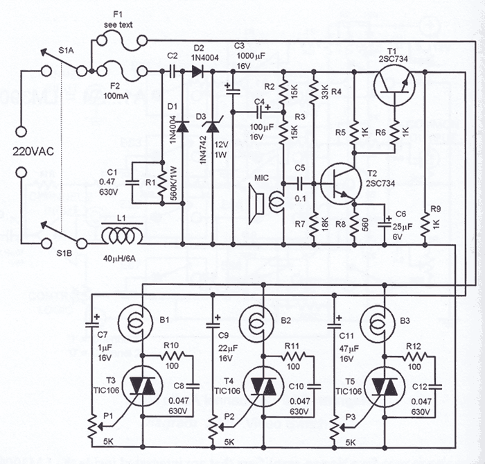
This sound-controlled lighting circuit design is utilized to adjust the brightness of connected lights in synchronization with captured sound. The sound-controlled lighting circuit operates by detecting audio signals through a microphone or sound sensor. The circuit typically consists of several...
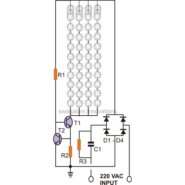
The circuit of a current-controlled LED tube light employs high-voltage transistors to implement the necessary current control operation based on a fundamental principle. A resistor (R2) is utilized to convert the increasing current into a voltage across itself. This...
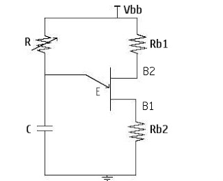
At the point Vp, the emitter triggers and turns the UJT (Uni-Junction Transistor) ON. Up to this point, the emitter is isolated and does not conduct, resulting in no current conduction between Base1 and Base2. The operation of the Uni-Junction...
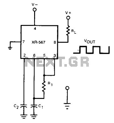
The frequency of the current-controlled oscillator can be doubled by feeding a portion of the square-wave output from pin 5 back to the input at pin 3. This configuration allows the quadrature detector to operate as a frequency doubler,...
Crystal radios have been around for over 100 years and exist in many different shapes, sizes, and complexities. Some are definitely better than others, but if wired correctly and connected to a good antenna and ground wire system, this...
A Pierce Oscillator is a type of oscillator that utilizes a crystal instead of a parallel-resonant circuit (LC circuit). This oscillator also employs the voltage developed from a tap between two capacitors in the tank circuit. Both Pierce Oscillators...