
a simple Astable Multivibrator with the help of a circuit diagram
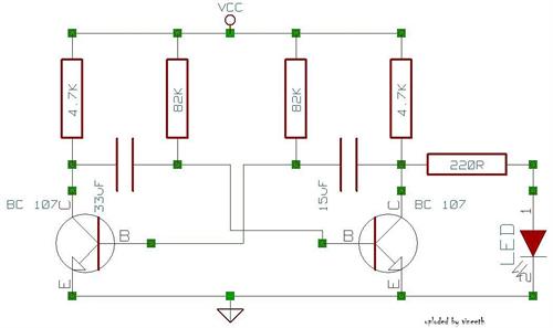
The astable multivibrator circuit typically consists of two NPN transistors, two resistors (R1 and R2), and two capacitors (C1 and C2). The configuration allows for continuous switching between the two transistors, creating a square wave output. The resistors R1 and R2 are connected to the collector terminals of the transistors, providing biasing and stability to the circuit. The capacitors C1 and C2 are crucial in determining the frequency of oscillation, as they charge and discharge, controlling the timing of the switching action.
In practical applications, the frequency of oscillation can be calculated using the formula:
\[ f = \frac{1.44}{(R1 + R2) \cdot (C1 + C2)} \]
Where:
- \( f \) is the frequency of the output square wave,
- \( R1 \) and \( R2 \) are the resistances in ohms,
- \( C1 \) and \( C2 \) are the capacitances in farads.
Additionally, the duty cycle of the output waveform can be adjusted by varying the values of the resistors and capacitors, allowing for flexibility in design based on specific application requirements. The astable multivibrator is widely used in applications such as clock pulses, tone generation, and timer circuits due to its simplicity and effectiveness in generating a square wave output.An Astable Multivibrator is a switching circuit which switches its output on and off for a designed time period. This article also describes about its working. An Astable Multivibrator or a free running oscillator circuit is generally used to generate square waves for a specified time period.
The name Astable Multivibrator is used for it because, it does not have a stable state and it switches between two quasi stable states. Consider the instant at which the DC supply is switched on. Even though, both the transistors are made of the same material their is a chance for disproportion among the two and That is the key to the generation of vibrations. This phenomenon is further enhanced by the transistor configuration as shown in the figure. The collector terminal of T1 is connected to the base of T2 via a capacitor C1 and similarly the collector terminal of T2 is connected to the base of transistor T1.
So, due to this configuration only one transistor can remain switched-on at a time. The time period is determined by the capacitor connected to its base. As said above, at the time of providing supply to this circuit, any imbalance among the transistors can cause any one of the transistor to conduct more, let it be T1 now. As T1 turns on its collector potential will be VCEsat which is approximately equal to 0. 3v therefore the transistor T2 will get a base potential less than the cutin voltage 0. 7 and this prevents transistor T2 from turning on. Now since the capacitor C1 is connected in series with the base terminal of T2, the capacitor charges to vcc through RC1 resistor.
As the capacitor charges, the base voltage of T1 increases exponentially and when it is more than 0. 7 v, the T2 turns on. But the collector voltage of T2 drops to VCEsat which in turn is connected to the base of T1 and it drives T1 to switched-off state. Now C2 charges to vcc through Rc2 resistor and when the base voltage of T1 is more than 0. 7v T1 turns on and T2 goes off. This regenerative action continues until the power supply is maintained. Thus the time period depends on the value of C1 and C2 This circuit can function as as per our design.
But, there may be some small variation subsequently, because of the approximation provided in the values of capacitor and resistors. in fact we used only standard valued components available in market. 🔗 External reference
Related Circuits
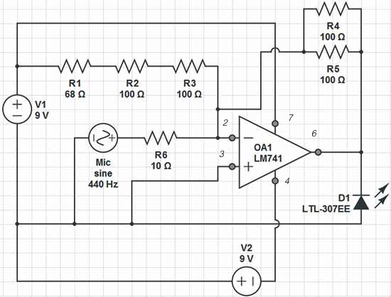
Red = V+, Black = V-, Green = GND, Yellow = Mic Input, Orange = LED Output. The op-amp used is an LM741, which is intended to adjust the peak brightness of the LED based on the ambient sound...

The FM Radio Receiver IC TDA 7012T is a straightforward component that offers excellent sensitivity and selectivity for FM radio reception. This single-chip FM receiver, known as IC TDA7012T, requires minimal additional components to construct an FM receiver. The...

Intended for a NiCad application, this charging circuit can be used with a wide range of batteries. A low-battery detector is included, and the trip voltage is set via a 500 kΩ potentiometer. Select the resistor for the battery...
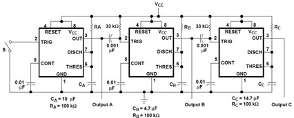
A sequential timer circuit device is utilized in various applications for initializing conditions during start-up or for activating test signals in sequences, such as in test equipment devices. The circuit diagram below illustrates a sequencer circuit with potential applications...
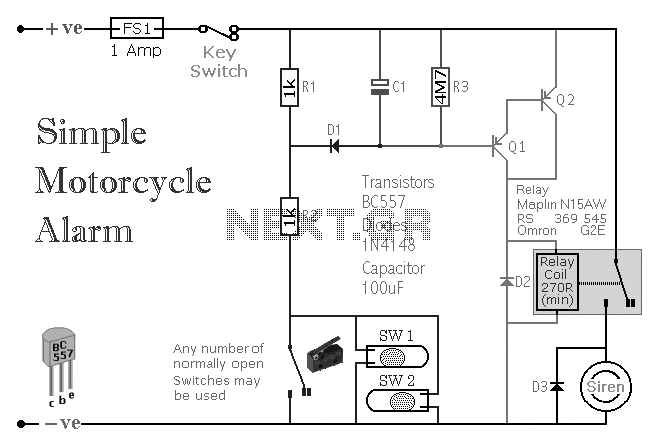
A simple transistor-based motorcycle alarm circuit. This circuit is easy to build and designed to operate at 12 volts. However, by replacing the relay with one that has a 6-volt coil, it can also provide protection at that voltage. The...

The figure illustrates a current boosting circuit configuration utilizing the PGA202 and OPA633 operational amplifiers. This circuit enhances the output current capability of the PGA202 operational amplifier, leveraging the performance characteristics of the OPA633 to achieve a higher output...
Warning: include(partials/cookie-banner.php): Failed to open stream: Permission denied in /var/www/html/nextgr/view-circuit.php on line 713
Warning: include(): Failed opening 'partials/cookie-banner.php' for inclusion (include_path='.:/usr/share/php') in /var/www/html/nextgr/view-circuit.php on line 713