
Active Power Factor Correction Circuit
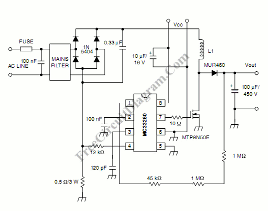
The power factor correction (PFC) circuit is a critical component in modern electronic systems, particularly for applications requiring efficient energy management and compliance with regulatory standards. The circuit typically begins with an AC input, which is rectified using a diode bridge to convert the AC voltage to DC. This process, while effective, can lead to significant harmonic distortion if not managed properly.
To mitigate this, the PFC circuit employs a boost converter topology. The boost converter consists of an inductor, a switch (usually a MOSFET), a diode, and an output capacitor. During the switch's ON state, current flows through the inductor, storing energy. When the switch is turned OFF, the inductor releases its stored energy to the load through the diode, which results in a higher output voltage than the input voltage. This operation not only increases the DC voltage but also shapes the input current to be more sinusoidal, thus improving the power factor.
The inclusion of inrush current detection is crucial for protecting the circuit during startup, preventing damage from sudden surges. Overcurrent protection ensures that the circuit operates within safe limits, while overvoltage and undervoltage protection circuits safeguard the connected load from voltage fluctuations.
The design also emphasizes the use of smaller inductors and MOSFETs, which contribute to a reduction in overall system size and cost. By optimizing component selection and layout, the PFC circuit achieves high efficiency and reliability, fulfilling the stringent requirements of energy regulations while minimizing operational costs.
Overall, the power factor correction circuit is essential for enhancing the efficiency of power conversion systems and ensuring compliance with international standards, making it a vital consideration in the design of modern electrical devices.Active power factor correction stabilize the electrical demand of a device to give the best power factor characteristic of many types of loads. To meet power factor regulation, a low cost solution should be designed. In many application, the need of high DC voltage is usually implemented by a direct rectification of the AC line followed by bulk ca
pacitor filtering. This capacitor filtering introduce current spike that distort the power line sine waveform, and this introduce a poor power factor, resulting in an apparent input power that is much higher than the real power. This can be solved by inserting a pre-regulation between the rectifier and the bulk capacitor. We call this pre-regulator circuit as power factor correction circuit. Here is the schematic diagram of the circuit: This power factor controller is a low cost system solution for boost mode follower.
that meets IEC1000 3 2 standard. This power factor correction circuit includes an inrush current detection, protection against overcurrent, overvoltage and undervoltage. Follower boost mode for system cost reduction smaller inductor and MOSFET can be used. [Circuit schematic source: ON Semiconductor Application Notes] We aim to transmit more information by carrying articles.
Please send us an E-mail to wanghuali@hqew. net within 15 days if we are involved in the problems of article content, copyright or other problems. We will delete it soon. 🔗 External reference
Related Circuits
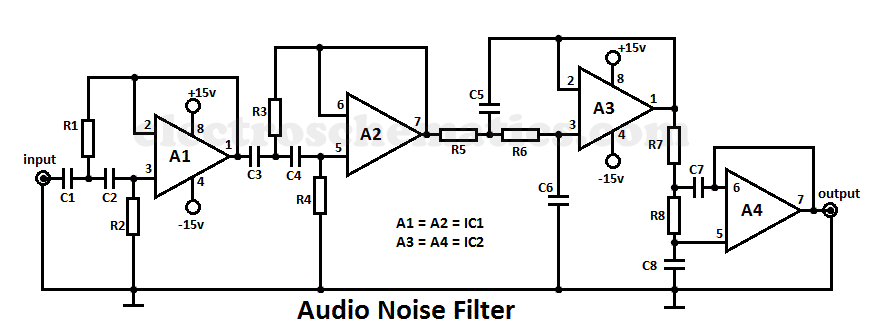
This audio noise filter circuit is a bandpass filter designed for the audio frequency range. It effectively filters out unwanted signals that fall below or above the audio frequency spectrum. The audio noise filter circuit operates as a bandpass filter,...
The schematic diagram of a 100-watt audio amplifier utilizing MOSFET technology. A comprehensive collection of electronic circuit diagrams is available, including a 100W RMS amplifier and a 0-30V stabilized variable power supply with current control. The 100-watt audio amplifier schematic...
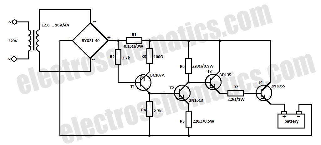
The car battery charging current is automatically limited to 4.2A. If there is a 600mV voltage on R1 (indicating 4A flowing through it), the T1 transistor begins to conduct. This prevents excessive charging current as the base current of...
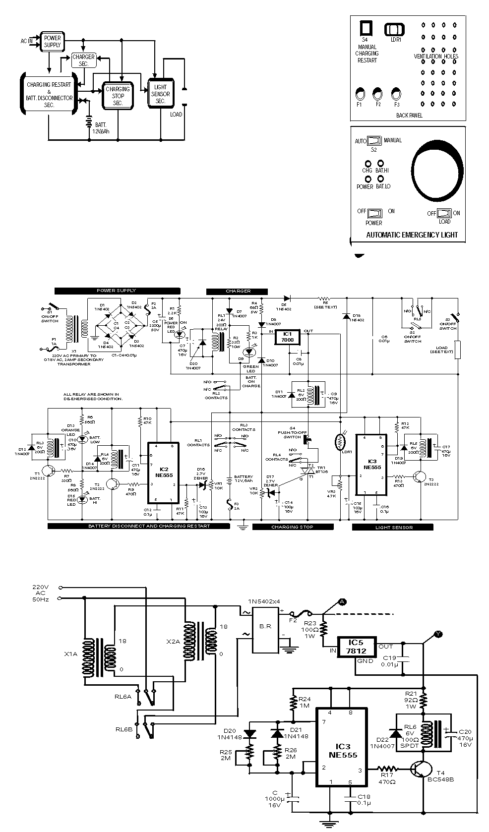
The circuit of automatic emergency light presented here has the following features: 1. When the mains supply (230V AC) is available, it charges a 12V battery up to 13.5V and then the battery is disconnected from the charging section....
In this circuit, a square wave is filtered using a high-order low-pass filter designed to eliminate most harmonics of the waveform at a -3 dB frequency. Consequently, the output of the filter is a fundamental sine wave. This technique...
DC power supply with a shunt, rectifier, filter, limiter, and regulator. The circuit is simple and cost-effective, capable of meeting the requirements. The 6.3V indicator lights HL1 and HL2 indicate the lathe's running and stopping status through a relay...
Warning: include(partials/cookie-banner.php): Failed to open stream: Permission denied in /var/www/html/nextgr/view-circuit.php on line 713
Warning: include(): Failed opening 'partials/cookie-banner.php' for inclusion (include_path='.:/usr/share/php') in /var/www/html/nextgr/view-circuit.php on line 713