
ADC 207 Flash Converting Schematic Diagram

The ADC 207 is designed for high-speed applications, leveraging the advantages of its Flash Converting architecture. This architecture allows for rapid conversion of analog signals to digital format, making it suitable for real-time processing tasks. The integration of the advanced 1.2-micron CMOS technology contributes to the device's efficiency and performance, enabling it to maintain linearity across its operating range.
The 128 auto-balanced comparators are a critical feature, as they help mitigate the impact of temperature variations and dynamic changes in the signal, ensuring consistent performance in varying conditions. The design includes a resistor ladder that is strategically configured to connect to an external voltage source, which plays a crucial role in establishing the reference levels required for accurate 7-bit linearity conversion.
The ADC 207's capability to operate at a frequency of 20 MHz allows for high-throughput applications, and the low power consumption of 250 mW makes it suitable for battery-operated devices or energy-sensitive applications. The minimal sampling time of 12 ns ensures that the ADC can capture fast-changing signals without significant delay, making it ideal for high-speed data acquisition systems.
The three output levels provided by the ADC 207 facilitate straightforward interfacing with various external components, enhancing its versatility in system design. This feature allows designers to easily integrate the ADC into different applications, whether in consumer electronics, industrial automation, or telecommunications, where precise analog-to-digital conversion is required. Overall, the ADC 207 stands out as a robust solution for high-speed digital signal processing needs.ADC 207 is the first to use Flash Converting An Advanced High Speed VLSI 1. 2 micron CMOS process. The process that is able to do the ADC 207 as mentioned earlier is very great and makes the ADC 207 is unique. The speed of the process of this ADC has a good linearity and have a stable temperature. ADC 207 has a lower power consumption is 250 mW. AD C is working with +5 VDC voltage source and at a frequency of 20 MHz. ADC 207 has a small sampling time is 12nS, thus making the ideal sampling results. ADC 207 has 128 features auto balanced comparators with each conversion that serves to offset temperature and dynamic effects that exist. Resistor ladder in the ADC 207 has a mid point that is connected to an external voltage source and function in the conversion of 7-bit linearity.
ADC 207 has 3 levels of output that is easy to connect it with external components. 🔗 External reference
Related Circuits
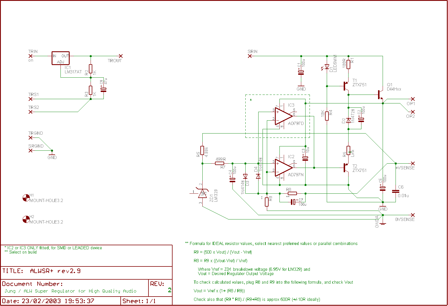
The reference selected is an LM329 sub-surface (or buried) zener (ZD1). While the circuit symbol resembles that of a zener diode, it functions as an active device, resulting in a significantly lower dynamic impedance of approximately 1 ohm compared...
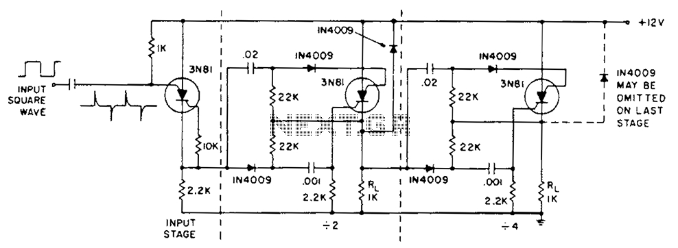
The circuit operation is initiated by a positive edge signal. The anodes of the triac switches are activated while the cathodes of the switches remain closed. A male-female IN4009 diode is utilized for positive transient suppression, ensuring that the...
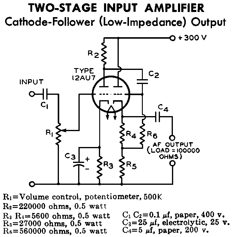
12AU7 (ECC82) Cathode Follower Tube Preamplifier Schematic. This is a two-stage 12AU7 preamplifier featuring a low impedance output stage. The overall gain is approximately 8 times. The 12AU7 (ECC82) tube is a dual triode commonly used in audio applications due...
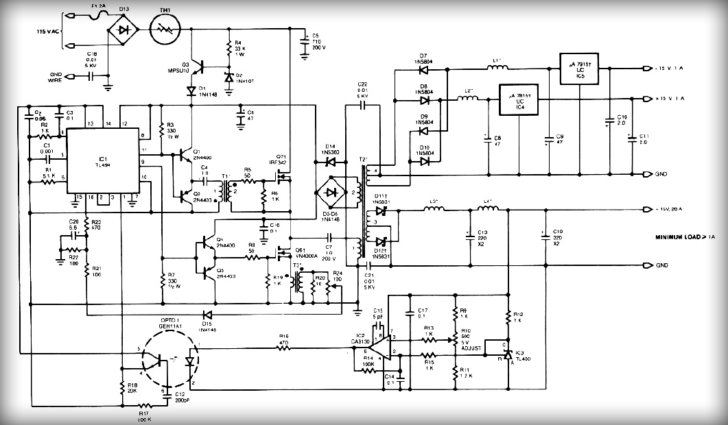
This power supply employs two VN400A 400-Volt MOSFETs arranged in a half-bridge configuration. The outputs provide +5V at 20A and +15V at 1A. Low-current outputs utilize three-terminal regulators, allowing for either 12 Volts or 15 Volts to be achieved...
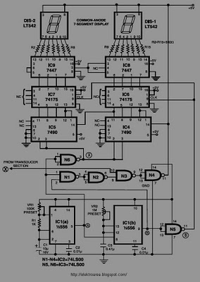
This circuit is designed to display the speed of a vehicle in kilometers per hour (km/h). An opaque disc is mounted on the spindle connected to the front wheel of the vehicle. The disc features evenly spaced holes along...
This application note demonstrates a simple 8-direction digital compass application utilizing Zilog's Z8 Encore!® MCU and an external compass sensor hardware. Communication ports are provided for the digital compass to receive commands and send status via the I2C bus...