
AF locked loop circuit diagram
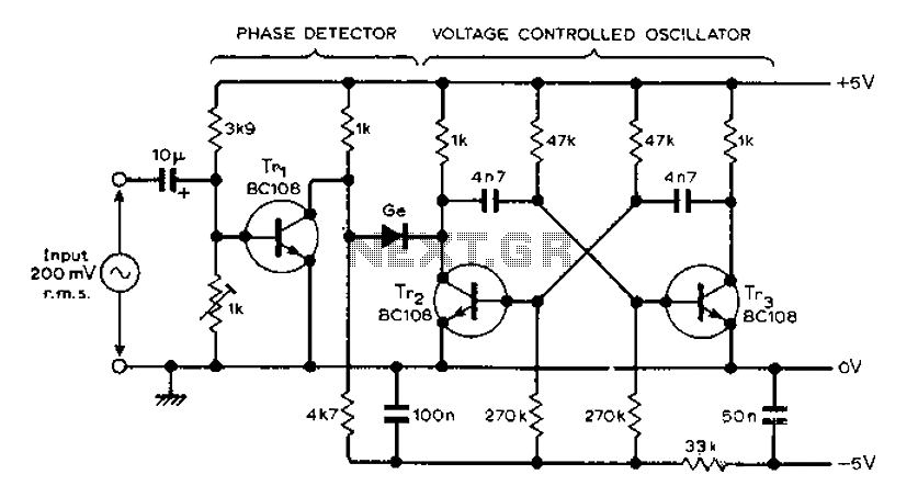
The MVBR circuit is designed to achieve phase locking by employing a two-transistor arrangement that serves as the core of the phase-locked loop. The functionality of the circuit hinges on the interaction between the voltage-controlled oscillator (VCO) and the phase detector. The VCO generates an output waveform that is subject to modulation based on the input signal frequency.
In this configuration, TR1 plays a crucial role by switching in response to the logic gate formed by the diodes. This switching action occurs during specific half cycles of the input waveform, allowing the circuit to effectively track the phase of the incoming signal. The diodes ensure that the transistors operate in the correct states, enabling the PLL to lock onto the desired frequency.
The phase detector's output is filtered to isolate the most negative phase of the waveform, which is critical for maintaining synchronization. This filtering process is essential for reducing noise and improving the stability of the phase-locked loop. The output of the phase detector is then used to adjust the frequency of the VCO, ensuring that it remains locked to the phase of the input signal.
Overall, the MVBR circuit exemplifies a straightforward yet effective implementation of a phase-locked loop, leveraging basic electronic components to achieve reliable frequency synchronization. The design is particularly useful in applications where precise timing and frequency control are required, such as in communication systems and signal processing. Circuit MVBR traditional two-transistor and other components to provide a simple phase locked loop. TR1 and diodes in the form of logic gate turns on, then half period and the VCO input waveform alternately respectively. Filtering process, the phase detector output is the most negative phase of the waveform.
Related Circuits
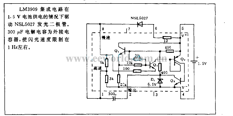
With a 1.5V battery supply, the integrated circuit LM3909 can drive the light-emitting diode NSL5027. The 300μF electrolytic capacitor acts as a timing capacitor, which limits the flash speed to approximately 1Hz. The circuit utilizes the LM3909, a popular LED...

The HA7210 oscillator, in conjunction with the IOL7642 quad CMOS operational amplifier, forms a sleep-mode control circuit. This circuit can enter sleep mode when a logic high is applied to the Reset input or through an RC timer that...

A quad op-amp serves as the core component of this function generator. U1A produces a square wave, which is outputted to J8. J1 and J2 are pulse outputs derived from differentiating the square wave. The integrator U1B creates a...
This document describes a simple triac tester circuit that can also be utilized for testing silicon-controlled rectifiers (SCRs) and both PNP and NPN transistors. The circuit operates on 3V DC, which can be derived from a Zener diode combined...
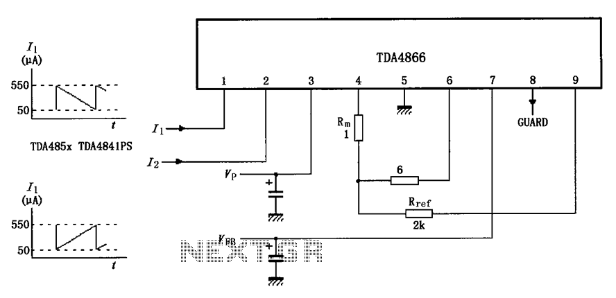
The TDA4866 test circuit operates with a positive supply voltage (VP) and a feedback voltage (VFB) in conjunction with a flyback circuit. The circuit responds to changes in the input signal, transitioning from one state to another. The input...
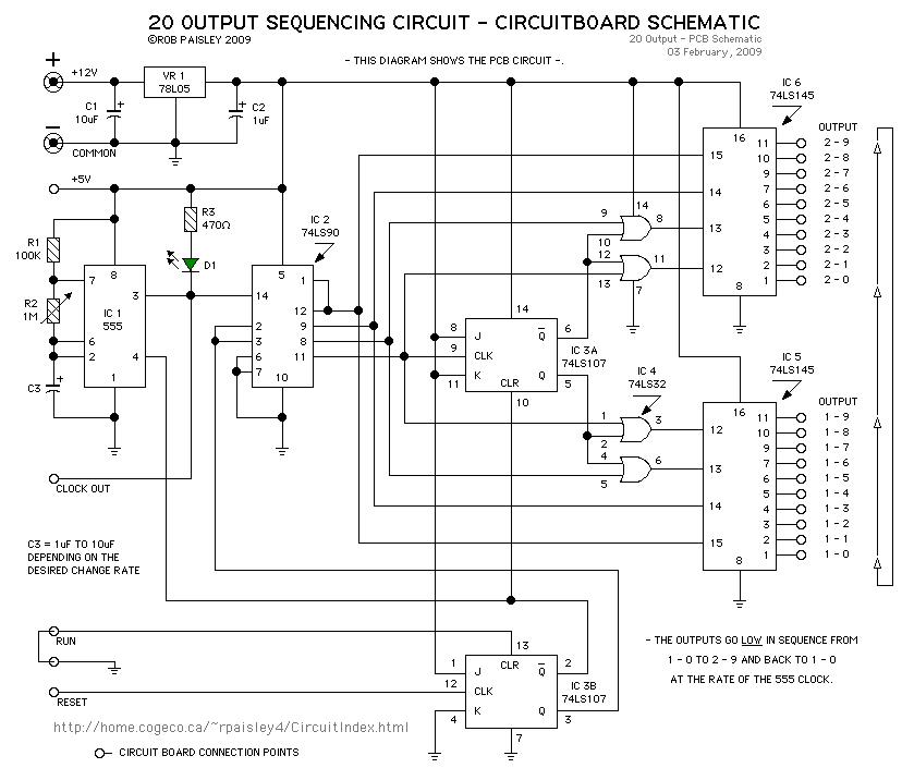
This page features a circuit that has twenty open collector outputs that turn on one at a time in a continuous sequential manner. The circuit utilizes the 74LSxx family of TTL integrated logic devices. The circuits are designed to...
Warning: include(partials/cookie-banner.php): Failed to open stream: Permission denied in /var/www/html/nextgr/view-circuit.php on line 713
Warning: include(): Failed opening 'partials/cookie-banner.php' for inclusion (include_path='.:/usr/share/php') in /var/www/html/nextgr/view-circuit.php on line 713