
AM Modulator
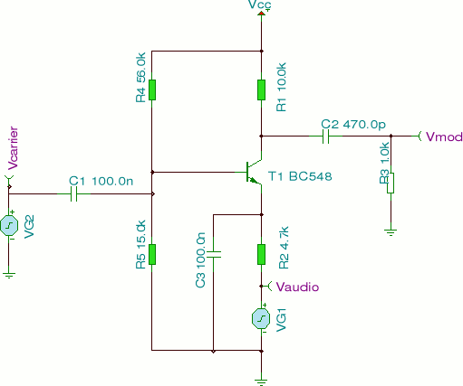
The circuit is designed to demonstrate amplitude modulation (AM) using two distinct signal generators. The first generator, VG2, produces a high-frequency RF carrier signal at 200 kHz, which serves as the primary signal for modulation. The second generator introduces a low-frequency audio signal at 1 kHz, which modulates the amplitude of the RF carrier.
The mixing of these two signals occurs within the transistor stage, specifically using a BC548 transistor, which is configured to amplify the combined signals. The output at the collector of the transistor is an amplitude-modulated signal, where the amplitude variations correspond to the 1 kHz audio signal, effectively encoding the audio information onto the RF carrier.
To eliminate any DC offset from the output, a coupling capacitor (C2) is employed in conjunction with a resistor (R3). This configuration ensures that only the varying AC component of the modulated signal is present across the load resistor R3, allowing for a clear observation of the AM waveform.
For simulation purposes, the circuit can be analyzed using Tina software, which provides a platform for visualizing the waveforms generated by the circuit. In addition, Spice Opus can be utilized for further simulation and analysis. Upon initiating Spice Opus and loading the vmod.cir file, users can execute commands to display the netlist, simulate the circuit, and visualize the output waveform.
The command sequence facilitates a comprehensive analysis of the circuit's performance, with specific emphasis on the AM wave characteristics observed at node 3. The limitation of the RF carrier frequency to 200 kHz is a strategic choice to simplify the simulation process, while the output waveform is designed to illustrate two complete cycles of the audio modulation, providing a clear representation of the system's functionality.This circuit uses two signal generators to simulate an Amplitude Modulated RF carrier wave. The output can be used to simulate the response of LC and tank circuits. Two signal generators are used in this circuit, one representing a high frequency (200kHz) RF carrier, VG2, the other signal generator is used to inject a 1KHz audio signal. The two si gnals are mixed and amplified by the transistor and an amplitude modulated signal appears at the collector of the BC548. The DC component is removed by C2 and R3 and the RF output now appears across the load resistor R3. Waveforms below are produced using Tina. To produce an output in Spice Opus start the program and load the new vmod. cir The modulated signal appears across R3 which is now node 3 and earth. After loading the circuit the command "listing" will display the netlist. The command "run" will then simulate the circuit, "display" will print a list of all variables in the circuit.
The command plot v(3) will display the AM wave between node 3 and 0 i. e. the load resistor R3. Note to speed up simulation, the RF carrier has been limited to 200KHz only, and the output waveform just shows two complete cycles of the audio wave, i. e. 2ms as the modulating frequency is 1k. There will be some spice tutorials shortly on my pages. 🔗 External reference
Related Circuits
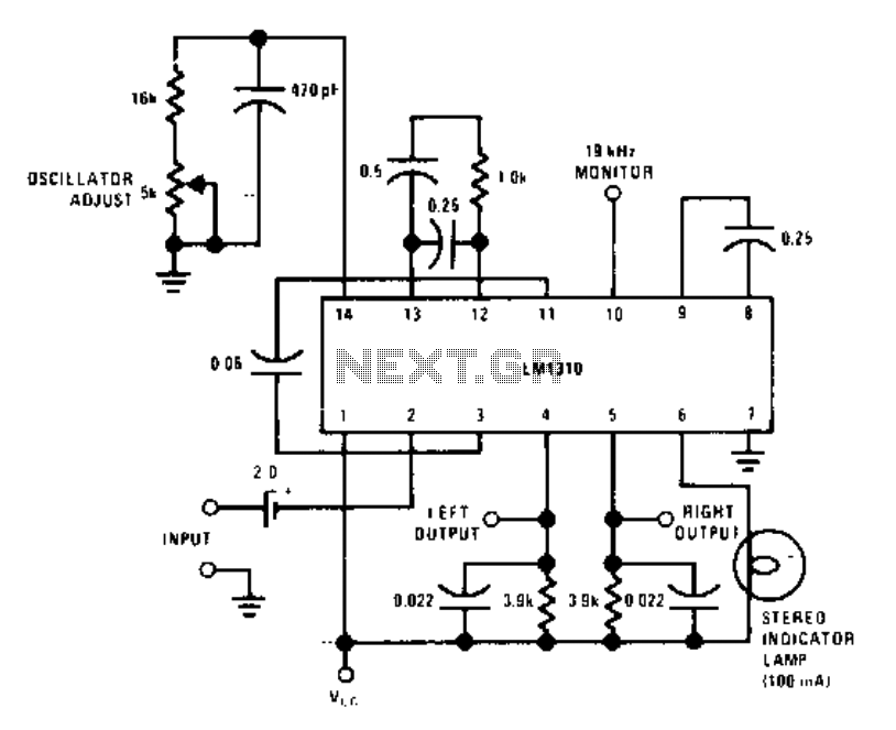
This circuit utilizes a single integrated circuit, the LM1310, to provide left and right outputs from a composite MPX stereo signal. The oscillator adjust resistor R1 is configured for 76 kHz, which corresponds to 19 kHz at pin 10....
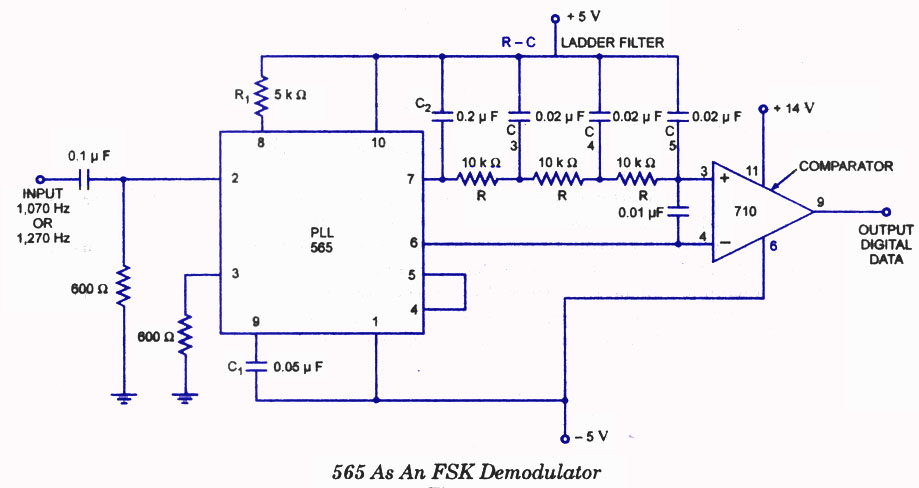
A highly effective application of the 565 Phase-Locked Loop (PLL) is its use as a Frequency Shift Keying (FSK) demodulator. In the 565 PLL, frequency shifting is typically achieved by driving a Voltage-Controlled Oscillator (VCO) with a binary data...
The TBA120 Series integrated circuits (ICs) offer a high-gain limiting intermediate frequency (IF) amplifier and a quadrature coincidence detector in a single package. These ICs are primarily designed for the extraction of television intercarrier sound, which is frequency modulated...
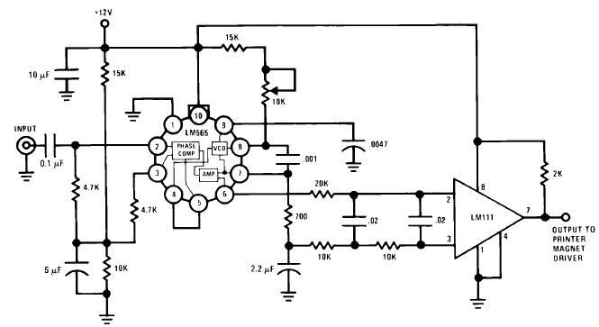
A simple Frequency Shift Keying (FSK) demodulator for 2025 Hz and 2225 Hz can be designed using the LM565, a general-purpose phase-locked loop integrated circuit. This IC includes a stable, highly linear voltage-controlled oscillator that provides low distortion FM...
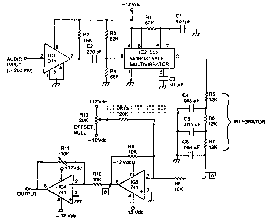
The circuit recovers an FM audio signal that varies from less than 1 kHz to about 10 kHz. The circuit is designed to demodulate frequency-modulated (FM) audio signals within the frequency range of less than 1 kHz to approximately 10...
With the impending shutdown of the 405-line transmitter network, individuals with collections of early television sets must find new methods to supply them with appropriate signals. Regardless of the scheme implemented, a method for converting baseband audio and video...