
Analog To Digital Converter

An Analog-to-Digital Converter (ADC) is a critical component in modern electronic systems, enabling the conversion of real-world analog signals into a format that can be processed by digital systems. The operation of an ADC involves sampling the analog input signal and quantizing it into discrete digital values.
For an 8-bit ADC, the output resolution is 256 discrete levels, allowing for a relatively coarse representation of the input signal. This is suitable for applications where high precision is not critical. In contrast, 12-bit ADCs offer 4096 levels of resolution, providing a finer granularity that is beneficial for applications requiring greater accuracy, such as audio processing, instrumentation, and control systems.
The Flash ADC method is characterized by its speed, as it can convert an analog signal to a digital signal in a single step. This is achieved through the use of multiple comparators, each of which compares the input signal against a specific reference voltage. The output from these comparators is then used to generate a digital output that represents the input signal. Flash ADCs are typically used in applications where speed is essential, such as in high-frequency signal processing.
On the other hand, the Successive Approximation method is more complex and slower than Flash ADCs but is favored for its simplicity in design and reduced component count. This method utilizes a binary search algorithm to zero in on the input signal's value. By starting with the MSB and working down to the LSB, the circuit can effectively narrow down the range of possible values until the most accurate representation of the input signal is found. The comparator's output guides this process, indicating whether the current approximation is too high or too low, allowing the system to adjust accordingly.
In conclusion, the choice of ADC architecture—whether Flash or Successive Approximation—depends on the specific requirements of the application, including speed, resolution, and complexity. Understanding these methods is essential for designing effective digital systems that interface with the analog world.ADC is a circuit formed in a single functioning chip to change analog signal becomes digital signal. In general we apply chip ADC 8 beet to change analog signal stretch 0-5 V becomes digital level 0-255 for ADC 8 beet. At the moment have also been in big supply ADC capable to work for data process 12 bits. To do converting there are two methods. F irst method is use a Flash ADC. This method also is recognized as parallel ADC as easiest circuit to be studied. This method formed by using a group of comparator comparing input signal to reference strain applies op-amp. Resistor applied Resistor must having high tolerance that more accurate. Second method is method Successive Approximation. This method applies approach successively to look for value that is most precise. This register calculates by trying to all bit values started from MSB and terminated with LSB. During calculation process, register will monitor comparator output to see if calculation of binary is less or bigger than input signal.
🔗 External reference
Related Circuits
Scopeclock is a user-friendly hardware device designed to enhance the functionality of X-Y capable analog oscilloscopes. This hardware allows for the conversion of an analog oscilloscope into a scope clock. The project was developed by a team at CEDT...
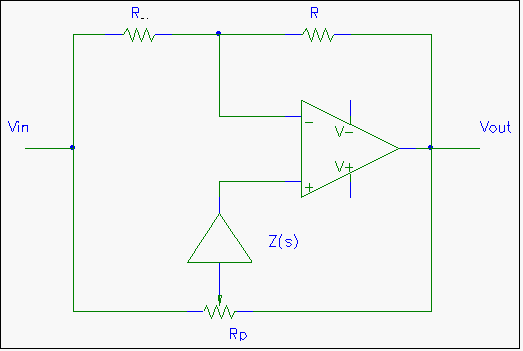
The time constant of R1C1 determines the low cutoff frequency, while the time constant of R2C2 determines the high cutoff frequency. The pass-band gain, Avpass = R2/R1. For a high-pass filter, Za must be capacitors and Zb resistors. By...
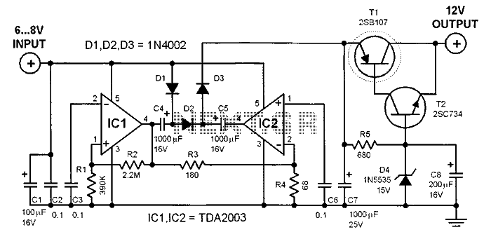
This 6V to 12V converter circuit is made with an IC from SGS with several additional components. The IC is a TDA2003 but it can be replaced with a TDA2002. The cost of building the 6 volts to 12...
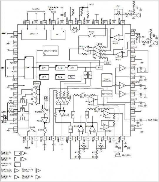
The BU8872 and BU8872FS are DTMF receiver integrated circuits designed for application in telephone answering machines, converting 16 distinct types of DTMF signals into 4-bit binary serial data. These receivers are available in a compact 8-pin DIP package (BU8872)...
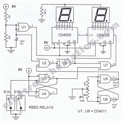
This digital DIY tachometer for bicycles utilizes two reed switches to gather speed information. The reed switches are positioned near the wheel rim, where permanent magnets, attached to the wheel spokes, pass by and activate the switches. The speed...
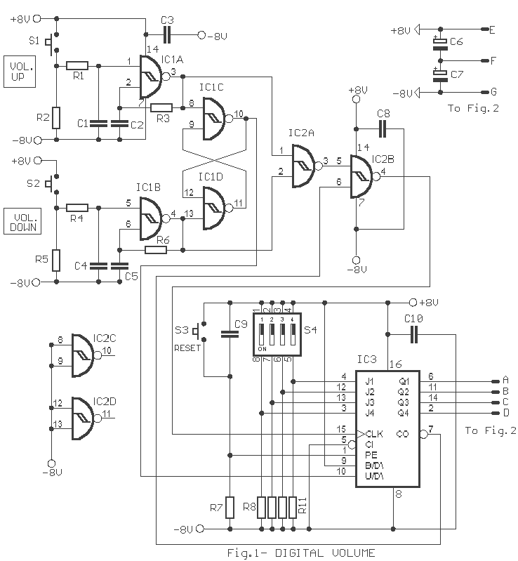
The circuit is a preamplifier with digital regulation intensity of sound. It is separated into three departments. The first schematic (Fig.1) shows the control circuit of the electronic potentiometer. The control is achieved through two pressing switches. The S1...