
Analog to Digital Converters
The ramp ADC is an older type that is rarely used today. It functions similarly to the successive approximation type but varies in the time required to capture a sample. A ramp ADC gradually increases the output voltage of its internal DAC until it matches the unknown voltage, at which point the comparator switches, sending a signal to the controller. The DAC input then becomes the ADC output. The time taken for the ramp to reach the unknown voltage can vary significantly based on its level. A ramp ADC with a more advanced logic controller can quickly transition to a successive approximation ADC.
The flash ADC consists of numerous comparators, one for each possible output value. For instance, an 8-bit flash ADC would require 256 comparators. While this may seem manageable with modern integrated circuit technology, a 32-bit flash ADC would necessitate approximately 3 billion comparators. Consequently, the cost of a flash ADC rises exponentially with the number of required comparators, making them uncommon above 16 bits. However, multiple flash comparators can be cascaded together. The primary advantage of flash ADCs is their extremely fast operation, approaching real-time performance. The only limitation on speed is the slew rate of the comparators used in their construction, allowing them to exceed 1 million samples per second.
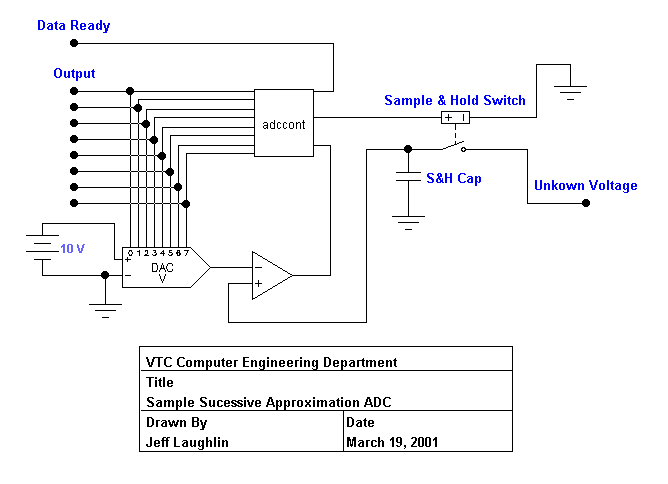
An important aspect of this schematic is the sample-and-hold (S&H) circuitry. During the analog-to-digital conversion, the DAC output is compared to the voltage across the S&H capacitor instead of directly comparing the DAC output to the input voltage. This design isolates the DAC from the input voltage, preventing interference in the conversion process due to significant fluctuations in the input voltage. The ADC controller signals a switch to close for a predetermined duration, allowing the capacitor to charge to the input voltage. After this period, the switch opens, and the ADC process begins. Although the capacitor discharges slightly during the ADC process, this is negligible due to the high input impedance of the comparator. The 10V source serves as a reference for the DAC.The successive approximation Analog to Digital Converter(ADC) is probably the most common ADC. It requires few parts, and is simple to operate. Also, it always takes exactly the same amount of time to calculate the result. In a nutshell, it consists of a comparator, a digital to analog converter(DAC), and a logic controller. The logic controller u ses the DAC to produce a voltage, and checks the output of the comparator to see if it`s over or under the unknown voltage. It then makes an adjustment, and checks again. It always takes exactly the number of steps that there are bits of resolution. IE, an 8 bit successive approximation ADC takes 8 steps to perform the conversion. A 16 bit ADC takes 16 steps, and so on. To be more specific, the controller first sets the most significant bit(MSB) of the DAC. This generates a voltage that is effectively half of the maximum output voltage. It then checks the output of the comparator. If the comparator indicates that the output of the onboard DAC is greater than the unknown voltage, the controller clears the MSB.
Otherwise it keeps the MSB set. Then it sets the second to most significant bit, and performs the same test. Each time that a bit is tested, the ADC gets half-way closer to the unknown voltage. In theory it will never quite get there, but in reality it gets there within our measurable margin of error. Once every bit on the input to the DAC has been tested, the input to the DAC becomes the output from the ADC!
In this way, the successive approximation ADC will always arrive at the most precise and accurate sample possible in the same amount of time. The ramp ADC: The older ramp type is no longer used, because it is functionally similar to the successive approximation type, but varies in the amount of time required to capture a sample.
A ramp ADC slowly raises the output voltage of it`s internal DAC, until the voltage reaches that of the unknown voltage, and the comparator switches, sending a signal to the controller. The input to the DAC is now the output of the ADC. Depending on the level of the unknown voltage, the amount of time it takes for the ramp to reach it can vary widely.
A ramp ADC with a smarter logic controller quickly becomes a successive approximation ADC. The flash ADC: The flash ADC consists of lots and lots of comparators, one for each possible output number. IE, if you have an 8 bit flash ADC, it will require comparators. That may not seem too bad, given modern IC technology. But a 32 bit flash ADC would require. 3 BILLION comparators! Because of this, the cost of a flash comparator goes up exponentially with the number of comparators required, and they are rarely seen over 16 bits.
Multiple flash comparators can be cascaded together, however. The great advantage of flash ADCs is that they are extremely fast, effectively real time. The only limit on their speed is the slew-rate of the comparators used to construct them. Because of this, they easily reach over 1 million samples per second. There is one part of this schematic that we haven`t discussed, and that is the sample & hold circuitry. When the analog to digital conversion takes place, the DAC output is compared to the voltage across the S&H capacitor rather than comparing the output of the DAC to the input voltage directly.
This isolates the DAC from the input voltage, and prevents the conversion process from getting messed up if the input voltage swings widely. The ADC controller signals the switch to close for a predetermined amount of time to allow the cap to charge up to the input voltage.
It then opens the switch, and begins the ADC process. Although the cap does discharge very slightly during the ADC process, it is negligible, due to the comparator`s very high input impedance. The 10v source is simply a reference for the DAC. In this case, it`s o 🔗 External reference
Related Circuits
There is no need to be disappointed the next time your digital camera displays a low battery indication during a picnic trip. Simply connect this digital camera adapter to the cigarette lighter outlet of your car and link the...
If a sensor is resistive, an alternating current (AC) is equivalent to pulsed direct current (DC), and the sensor will degrade based on the root mean square (RMS) value of the AC signal. Applying 1V AC RMS is effectively...
The analog to digital sketches have been extensively covered using various components. To progress to more complex circuits and concepts, it is essential to understand these simpler ones. This tutorial will not delve as deeply as others due to...
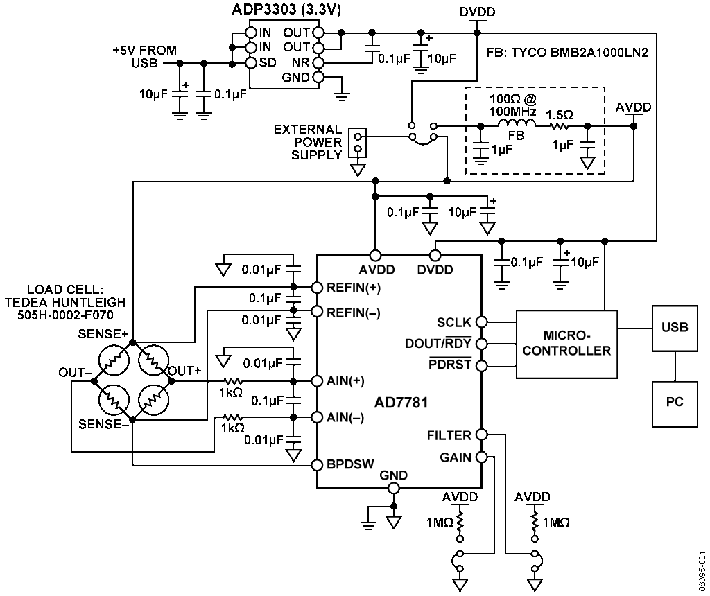
The AD7781 is a complete low-power front-end solution for bridge sensor products, including weigh scales, strain gauges, and pressure sensors. It contains a precision low-power 20-bit sigma-delta ADC, an on-chip low-noise programmable gain amplifier (PGA), and an on-chip oscillator....
Questions frequently arise regarding the use of solar panels to power Fiber-To-The-Home (FTTH) equipment. This concept may seem unusual at first, but it is a practical solution for numerous businesses and municipalities. For instance, many municipalities have water towers,...
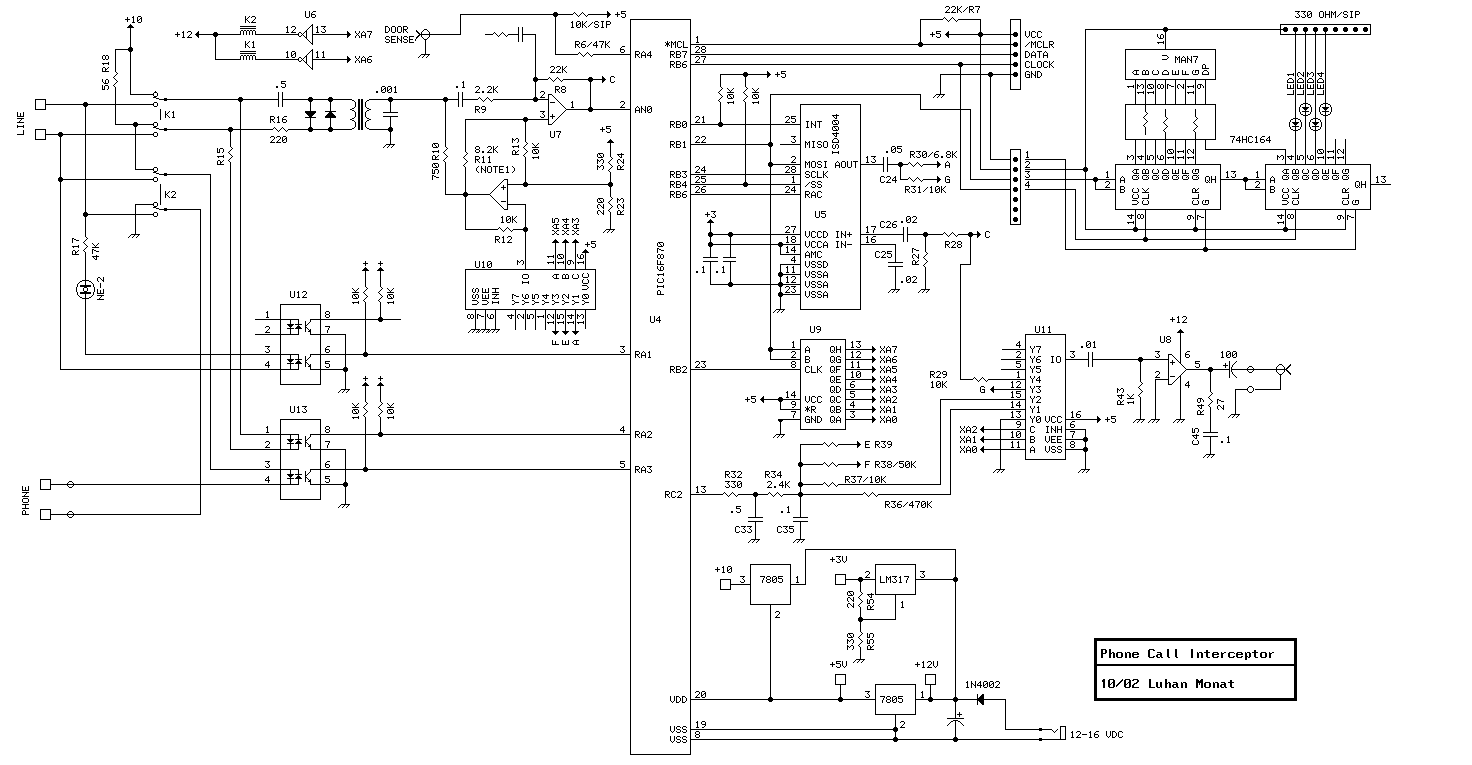
This unit is an upgrade of the previous phone call interceptor. Instead of using an answering machine to provide the outgoing message and recording functions, it uses the ISD4004 (from Windbond Electronics). The ISD4004 records up to 8 minutes...
Warning: include(partials/cookie-banner.php): Failed to open stream: Permission denied in /var/www/html/nextgr/view-circuit.php on line 713
Warning: include(): Failed opening 'partials/cookie-banner.php' for inclusion (include_path='.:/usr/share/php') in /var/www/html/nextgr/view-circuit.php on line 713