
Analogue to Digital Converter
A common inquiry is whether a serial ADC can be connected to a computer's serial port. The answer is affirmative, although simpler interfacing methods exist. The computer's RS-232 port operates at higher voltage levels, which are generally incompatible with most ADCs that use TTL/CMOS logic. Additionally, the asynchronous nature of the RS-232 serial port imposes further requirements on communication, including additional handshaking control lines. Furthermore, both ends of the link must be set to the same baud rate. In contrast, the A/D converter's serial port is synchronous, requiring minimal handshaking, typically just one wire for clock and one or two for data. If one is determined, it is possible to use the RS-232 port's handshake lines for bit-banging. This circuit employs such a control method.
Signal voltage conversion from the RS-232 port to the IC input pins is achieved through a combination of series resistors and the IC's internal input protection diodes. The output from this A/D converter can generate signals that are detected by the RS-232 port; while the output does not strictly adhere to RS-232 specifications, it has been observed to function correctly with the tested PC serial ports.
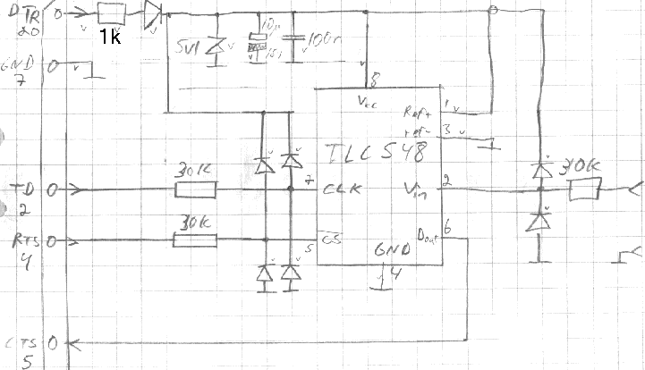
The circuit diagram displays the configuration, with the pin numbers corresponding to a 25-pin serial port connector. All diodes used are IN4148 or similar, and all resistors connected to the IC are 30 kOhm, serving to protect the IC inputs against overvoltage via the diodes. A power supply circuit is formed using a 1 kOhm resistor, one diode, a 5.1V zener diode, a 10µF capacitor, and a 100nF capacitor, drawing power from the serial port's Data Terminal Ready (DTR) pin.
The signal diagram indicates the necessary signals for controlling the TLC548 A/D conversion chip, which requires a chip select (CS) and an I/O clock signal (CLK) for operation. The chip outputs conversion results from its data output pins (Dout). These signals are straightforward and can be easily generated using simple software routines. While there are variations among different types of A/D converters, the principles demonstrated in this circuit can be adapted for interfacing other A/D converters to a PC.
A simple program for testing and operating the A/D converter circuit is provided, written in Turbo Pascal version 4.0, with compatibility for newer versions. The program requires the user to specify the I/O address of the PC's COM port in the source code before execution. For faster computers, a delay may be necessary after I/O access.
```pascal
Program serial_adc;
Uses Crt;
Const
combase = $2f8; { I/O address of the COM port used }
MCR = combase + 4;
LCR = combase + 3;
MSR = combase + 6;
Procedure Initialize_converter;
Begin
Port[MCR] := 3; { Power the DTR line and set CS input of chip to high }
Port[LCR] := 0; { Set clock line of the chip to low }
End;
Function Read_value: byte;
Var
value: byte;
count: byte;
Begin
value := 0;
Port[MCR] := 1; { Set CS low }
For count := 0 to 7 Do
Begin
value := value SHL 1; { Shift value left by 1 }
Port[LCR] := 64; { Set clock line high }
If (port[MSR] and $10) = $10 Then
Inc(value); { Increment value if the MSR indicates a high signal }
End;
End;
```
This program serves as a basic framework for interfacing the ADC with a PC, allowing for the reading of analog values through the serial port.This circuit is a simple 8-bit analogue to digital converter circuit which is connects to PC serial port. The circuit is based on TLC548 A/D-converter chip (might be hard to get nowadays, Texas Instruments makes this IC), which is an A/D-converter with serial output.
The output of the TLC548 is not directly suitable for standard serial data recept ion, so this circuit uses serial port handshaking lines in a nonstandard way which enables the communication between computer and converter chip to be implemented with as few components as possible. The circuit takes all the power it needs from PC serial port. A generally asked question is "Can I Connect a Serial A/D to My Computer`s Serial Port ". The answer to this question is yes, but there are simpler ways to interface to a computer. To begin with, the computer`s RS-232 port uses higher voltage levels that are incompatible with most ADC`s TTL/CMOS logic.
Another problem is that the computer`s RS-232 serial port is asynchronous, which places a few more requirements on the communication, including some additional handshaking control lines. Also, with the RS-232 serial port, you must set both ends of the link to the same baud rate. The A/D converter`s serial port is synchronous; thus, its handshaking requirements are minimal and it only requires one wire for clock and one or two wires for data.
If you are truly determined, you can bit-bang using the RS-232 port`s handshake lines. This circuit uses this control method. The voltage conversion of signals from RS-232 port to IC input pins is done using a combination of series resistors and the internal input protection diodes in the IC. The output of this A/D was able to directly output signals which seemed to be detected by RS-232 port (the output of the chip does not meet RS-232 specifications, but in practice still worked with the PC serial ports tested).
The picture below is tha circuit diagram of the circuit. The pin numbers of the connector are pin numbers of 25-pin serial port connector. All diodes are IN4148 or similar. All resistors connected to IC are 30 kOhm and their function is to protect the IC inputs with the diodes against overvoltage. The 1 kOhm resistor, one diode, 5. 1V zener-diode, 10uF and 100nF capacitors make the power supply which takes circuit power from serial port Data Terminal Ready -pin.
The following signal diagram tells that signals are needed for controlling the TLC548 A/D conversion chip. The chip needs chip selected (CS) and i/o clock signal (CLK) to operate. The chip gives the conversion results from data output pins (Dout). Those signals are simple and easy to understand and can be easily generated using simple software routine.
This type of signaling is quite common in many A/D converters with serial outputs. There are differences in different type of A/D converters, but you can easily use the ideas used in this circuit for interfacing other types of A/D converters to your PC. Here is a simple program for testing and operating A/D converter circuit. The program is written using Turbo Pascal version 4. 0 and can be compiled with never versions also. This program needs to know the address of your PC`s COM-port and you have to set it to the source code before running it.
If you have very fast computer, you might have to add some delay after if I/O access. Program serial_adc; Uses Crt; Const combase=$2f8; { I/O address of the COM port you are using } MCR=combase+4; LCR=combase+3; MSR=combase+6; Procedure Initialize_converter; Begin Port[MCR]:=3; { make DTR line to supply power and set CS input of chip to 1 } Port[LCR]:=0; { set clock line of the chip to 0 } End; Function Read_value:byte; Var value:byte; count:byte; Begin value:=0; Port[MCR]:=1; { set CS down } For count:=0 to 7 Do Begin { do the bit value eading 7 times } value:=value SHL 1; { value=2*value } Port[LCR]:=64; { clock line up } If (port[MSR] and $10)=$10 Then Inc(value); { read 🔗 External reference
Related Circuits
555 timer circuits LM555 - Astable Oscillator Calculator, Capacitor Calculator, Basic Circuits for the LM555 Timer, Triggering and Timing Helpers for Monostable Timers, Controlling Circuits for LM555 Timers, Advanced Circuits for the LM555 Timer, LM556 Timers with Complementary or...
This document serves as a resource for developers who are new to Texas Instruments (TI) ARM-based processors, as well as for seasoned developers seeking to deepen their understanding of the different ARM architectures. It starts with an overview of...
This fixed-frequency triangular waveform generator, driven by a TTL square wave, produces triangular waveforms with a peak-to-peak voltage of typically 16 V at frequencies reaching several MHz. The design utilizes a single AND open collector gate or an open...
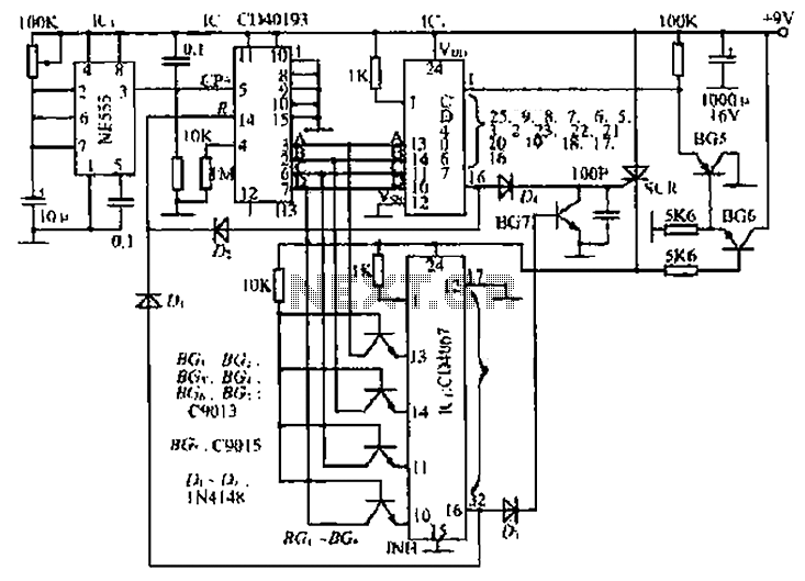
The circuit consists of an oscillator, a counter, and an Iseki circuit divided into three parts. The oscillator is based on the NE555 timer and several external RC components, generating a pulse signal for the counter. The instantaneous power...
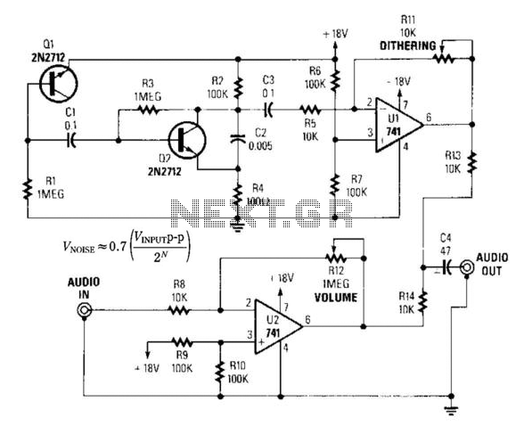
By introducing a small amount of noise to a signal intended for digitization (approximately 0.7 bits), where n represents the number of bits, for instance, an 8-bit signal with a peak-to-peak voltage of 2 V would result in a...
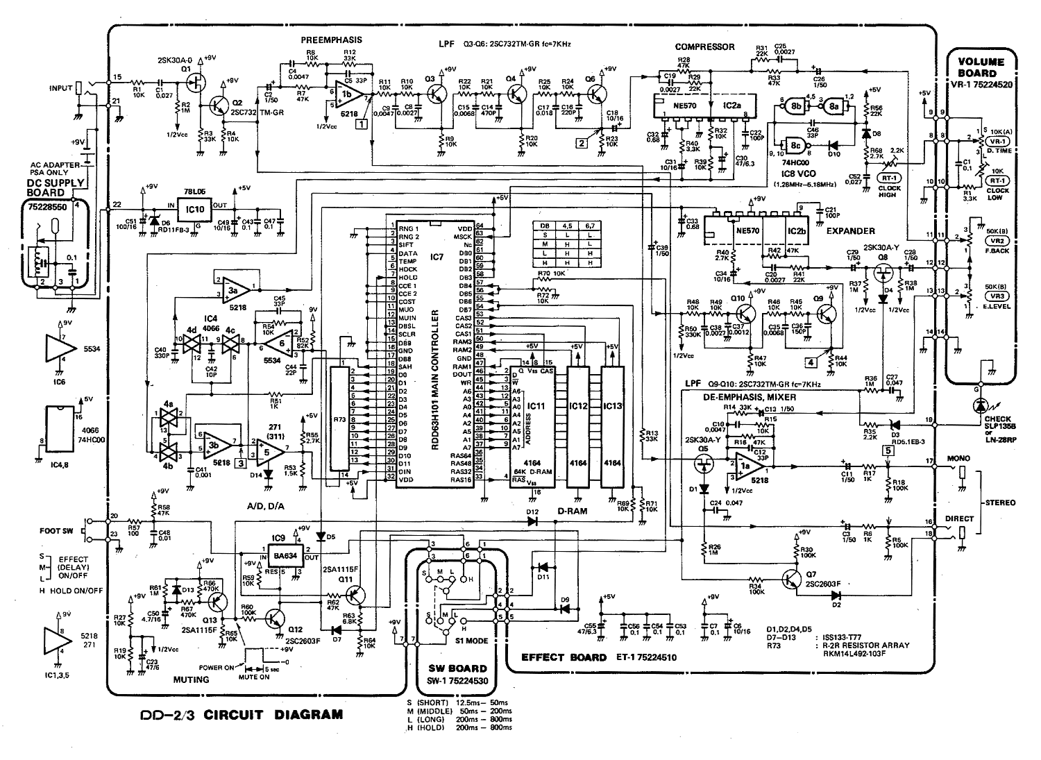
The DD-2 is a highly regarded digital delay pedal that emulates an analog sound. It was initially sold from 1983 until it was discontinued in 1986, after which it was relaunched without any modifications as the DD-3 (noting that...