
audio circuits 20

The single-stage virtual earth amplifier circuit operates by leveraging the characteristics of a field-effect transistor (FET) to achieve dynamic gain control. The FET's drain-source resistance plays a crucial role in determining the gain, which is influenced by the linearization provided by resistors R1, R2, and R3. These resistors ensure that the FET operates within a linear range, allowing for predictable performance in response to input signals.
The precision rectifier and peak detector work together to extract a control voltage from the output signal, which is essential for the compressor's operation. The adjustable attack and decay times, set by resistors R4 and R5, respectively, allow for fine-tuning of the circuit's response to varying signal amplitudes. The specified time constants of 1 ms for attack and 517 ms for decay provide a balance between responsiveness and stability.
The inclusion of a two-way switch adds versatility, enabling the circuit to function as either a compressor or a fixed-gain amplifier. This flexibility is further enhanced by the use of a potentiometer, which allows for manual adjustment of the control voltage, effectively acting as a gain or volume control.
The circuit design incorporates components that may be considered outdated by modern standards, such as germanium diodes and the 741 operational amplifier. However, the fundamental principles of operation remain relevant, and alternative components, such as the LF353, can be employed to improve performance.
The full-wave rectification process is critical for generating the control voltage, and the precision absolute value circuit referenced in the literature provides a reliable method for this function. The importance of matched resistors in ensuring consistent performance cannot be overstated, as variations in resistor values can lead to significant deviations in circuit behavior.
In summary, this circuit exemplifies a classic approach to dynamic gain control in audio applications, with a focus on maintaining linearity and optimizing response times. While it may not meet contemporary high-fidelity standards, it serves as a foundational design that illustrates key concepts in amplifier and compressor circuit design.The gain of the single stage virtual earth amplifier IC1 is determined by the drain-source resistance of the f. e. t. Resistors R1, R2 and R3 linearise the f. e. t. `s V-I characteristic. A control voltage is derived from the output signal by using a precision rectifier and peak detector.
Attack and decay times are adjustable by resistors R4 and R5, an d with the values shown give time constants of 1 and 517ms respectively. The two way switch allows the compressor to act as a conventional fixed-gain amplifier by applying a fixed control voltage (which may be varied with the potentiometer which could be used as a gain or volume control). The original publishers made an error in the circuit diagram and although this was pointed out to them at the time (but only after it was published I wasn`t sent any proofs and even had to buy my own copy of Wireless World to see my work) I do not know if a correction was subsequently published.
This is now a very old design (the diodes are germanium point contact types and the amplifiers are good old 741s); I would not go about this sort of circuit design in the same way today. Incidentally, this article is the first thing I had published (and I found when looking up the manuscript that I was paid the fee of £10 for my efforts which seemed a lot of money at the time).
The key component is the 2N3819 JFET which is used as a voltage controlled resistor the output of the circuit provides the control voltage which is derived by full-wave rectification followed by a peak detector. The full-wave rectifier (more properly called a precision absolute value circuit can be found in Tobey, Graeme and Huelsman`s: Operational Amplifiers (1971) page 249).
The circuit requires several matched resistors for correct operation and alternative versions of this sub-circuit, which require fewer matched resistors and overall fewer components, could be advantageously substituted. The full-wave rectifier shown will work with silicon diodes but it may be that substituting a silicon diode for D1 in the peak detector may alter the characteristics of the compressor; this could occur because of the greater forward voltage drop (0.
7V rather than 0. 2V) of silicon diodes. However, because the circuit operates in a closed-loop mode (which means that the gain is adjusted automatically to hold the voltage on the 4. 7 µF capacitor approximately constant) the overall effect of the extra voltage drop will be reduced and so the effect of the substitution may be negligible.
More modern op-amps such as LF353 (which are 8-pin duals) could be used instead of the 741s. The f. e. t. is operated in its so-called triode region` but without R1 and especially R2 and R3 its drain-source resistance would be non-linear (i. e. it would not obey Ohm`s Law or to put it another way: the value of rdswould be dependent on vds). Explanationofthelinearisationprocess. The attack time constant is determined by the product of R4 and the 4. 7 µF capacitor. When the input signal drops D1 becomes reverse biased and the decay time constant is determined by R5.
(Since the original publication date I have discovered that the termrelease`is used rather thandecay`in the case of compressors. ) Both time constants are something of a compromise the attack must be fast if the start of high amplitude signals are not to be overloaded until the gain reduces and the decay must be fast enough to allow low amplitude signals shortly following high amplitude ones to be given sufficient gain.
A problem arises after long periods of silence or low amplitude inputs the next high amplitude signal will get the full gain treatment` and so will initially overload the circuit and some distortion will be result. The best that could be done under these circumstances would be to reduce R4 to zero resulting in minimal attack time (determined by the maximum output current of IC3).
The circuit is by no means hi-fi` but will 🔗 External reference
Related Circuits

The oscillator circuit employs a center-tapped transistor output transformer that functions as a load for the collector of Q1, provides a feedback signal to the base, and acts as the output winding to drive the speaker. Resistor R1 supplies...
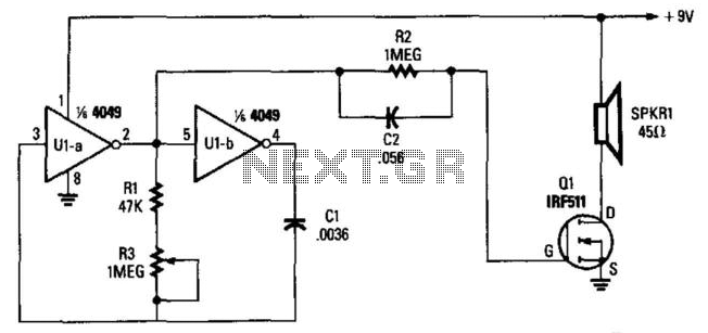
Two gates, U1A and U1B, of a 4049 hex inverter, are connected in a VFO circuit. Components R1, R3, and C1 set the frequency range of the VFO. With the given values, the circuit's output can range from a...

Almost any transistor will work. R1 and C1 will vary the tone. The circuit utilizes a transistor as the primary active component, which can be substituted with various types of transistors, including bipolar junction transistors (BJTs) or field-effect transistors (FETs)....
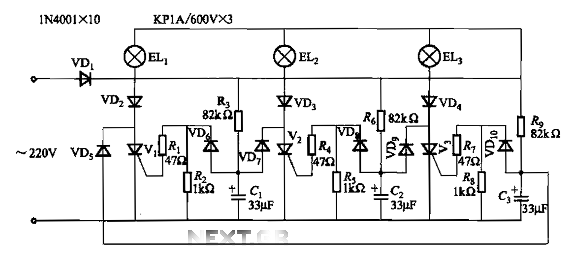
The circuit operates with a 220V mains supply through a diode (VDi) configured as a half-wave rectifier. Capacitors C1 to C3 are charged, and due to the lack of full synchronization in the charging process, a pilot thyristor is...
This circuit operates on 12V DC instead of mains AC. This is an advantageous approach for those who prefer not to deal with circuits connected directly to mains voltage or wish to power the stroboscope using batteries. Flash Slave...
Create a repository of circuits and service data for vintage valve and transistor radios. While many resources are available online, they often come at a cost. The intention is to share circuits and manuals with others rather than profit...