
Audio noise generator
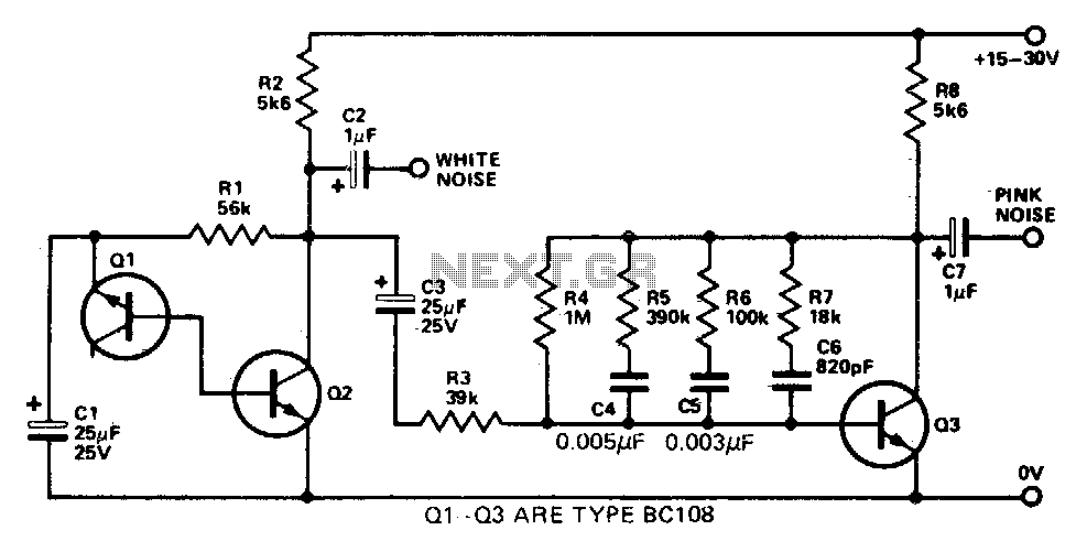
This circuit operates on the principle of generating noise signals, utilizing transistors for amplification and filtering. The first stage involves Q1, which is configured to exploit its zener breakdown characteristics to produce white noise. The reverse-biasing of the base-emitter junction allows it to enter zener breakdown at a specified voltage, generating random noise due to thermal agitation and avalanche effects within the semiconductor material.
The generated white noise, characterized by a flat spectral density across frequencies, is then directed to the base of Q2. This transistor acts as a buffer, providing an output voltage of approximately 150 millivolts. The output at this stage retains the characteristics of white noise, which is suitable for further processing.
To achieve pink noise, which has equal energy per octave, a filter is implemented to attenuate higher frequencies. This filter is designed to provide a 3 dB reduction in amplitude for each octave increase in frequency, effectively shaping the noise spectrum to the desired pink noise profile. The filter's role is crucial, as it modifies the white noise signal to meet the requirements of applications that benefit from pink noise, such as audio testing and sound masking.
Given that the filtering process can significantly reduce the signal amplitude, an amplification stage is necessary to restore the output level. Q3 is introduced as an amplifier, with the pink noise filter strategically connected in a feedback configuration between its collector and base. This arrangement allows for precise control over the gain characteristics of the amplifier, ensuring that the output maintains the desired pink noise characteristics while compensating for any attenuation introduced by the filter.
The final output from Q3 is thus a robust pink noise signal, which can be utilized in various applications. The output socket is designed to interface with external devices or systems that require pink noise input, facilitating its use in practical scenarios such as audio engineering, acoustics research, and sound design. Overall, this circuit exemplifies a straightforward yet effective design for generating and processing noise signals.This simple circuit generates both white and pin noise. Transistor Q1 is used as a zener diode. The normal base-emitter junction is reverse-biased and goes into zener breakdown at about 7 to 8 volts. The zener noise current from Q G flows into the base of Q2 such that an output of about 150 millivolts of white noise is available.
To convert the white noise to pink, a filter is required which provides a 3 dB cut per octave as the frequency increases Since such a filter attenuates the noise considerably an amplifier is used to restore the output level. Transistor Q3 is this amplifier and the pink noise filter is connected as a feedback network, between collector and base in order to obtain the required characteristic by controlling the gain-versus-frequency of the transistor.
The output of transistor Q3 is thus the pink noise required and is fed to the relevant output socket. 🔗 External reference
Related Circuits
White noise (the sound you hear when a TV is tuned to a non-existent station) has a frequency characteristic which raises the power level by 3dB with each increasing octave, and is not suitable for response testing (and will...

Almost any transistor will work. R1 and C1 will vary the tone. The circuit utilizes a transistor as the primary active component, which can be substituted with various types of transistors, including bipolar junction transistors (BJTs) or field-effect transistors (FETs)....
The air-cored inductor L1 is constructed using 13 turns of 1mm diameter enamelled copper wire, featuring an inner diameter of 10mm. The completed inductor is positioned over R7, with its terminals soldered to those of the resistor. All electrolytic...
A common telecoil follows the MM formula (magnetic-acting) and has an impedance of approximately 600 ohms to effectively receive signals. It is necessary to reduce the impedance in the high-frequency segment, which is achieved by placing a 150pF capacitor...
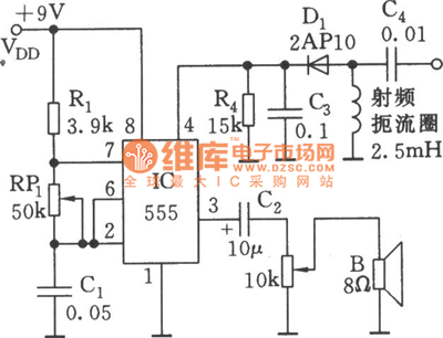
As shown in the figure, the 555 timer, resistors R1, RP1, and capacitor C1 form a controlled audio oscillator. The frequency of the oscillator is given by the formula f = 1.44 / ((R1 + 2 * RP1) *...
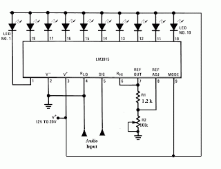
This meter circuit utilizes a single integrated circuit (IC) and a minimal number of external components. It displays audio levels using ten light-emitting diodes (LEDs). The input voltage can range from 12V to 20V, with a recommended voltage of...