
Audio Power Amplifier Circuit
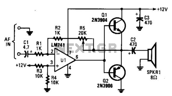
The circuit operates by utilizing the LM741 op-amp in an inverting configuration, which allows for signal inversion and amplification. The input signal is fed into the inverting terminal of the op-amp, while the non-inverting terminal is grounded. The feedback loop, which includes the base-emitter junctions of the complementary transistors, plays a crucial role in stabilizing the output and minimizing distortion during the transition between the on and off states of the transistors.
The inclusion of the potentiometer R5 enables the user to finely tune the gain of the amplifier. By adjusting R5, the feedback resistance changes, thereby altering the gain according to the formula for an inverting amplifier, which is given by -Rf/Rin, where Rf is the feedback resistor and Rin is the input resistor. This flexibility allows for a wide range of gain settings, accommodating various application requirements.
For enhanced thermal management and efficiency, the transistors Q1 and Q2 can benefit from the addition of a heatsink. This is particularly important when the circuit is required to deliver higher power levels, such as the maximum output of 0.5 W. The heatsink dissipates excess heat generated during operation, thereby ensuring reliable performance and longevity of the components.
In summary, this circuit effectively combines an LM741 op-amp with complementary transistors to create a versatile amplifier capable of driving loads while minimizing distortion and allowing for adjustable gain. The thoughtful design considerations, including the feedback loop and thermal management, contribute to its overall effectiveness in various electronic applications. The circuit, built around an LM741 op amp configured as an inverting amplifier, is used to drive complementary transistors (Ql and Q2). The op amp`s feedback loop includes the base-emitter junctions of both transistorsan arrangement that helps to reduce crossover distortion that would normally occur as-a result of the emitter-to-base junction voltage drop of about 0,6 V.
Potentiometer R5 varies the amplifier`s voltage gain from 1 to about 20. As much as 0.5 W can be obtained from the circuit if a heatsink is added to the transistors. 🔗 External reference
Related Circuits
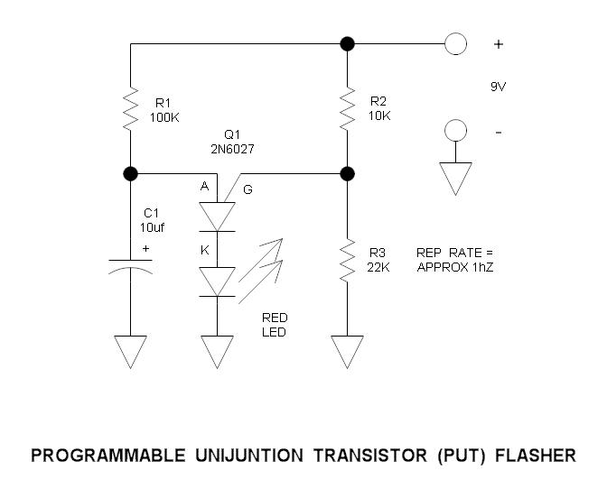
This is a simple circuit that illustrates the function of the programmable unijunction transistor. It can be quickly wired on a proto-board. The circuit utilizes a programmable unijunction transistor (PUT) to demonstrate its operation as an oscillator. The PUT, which...
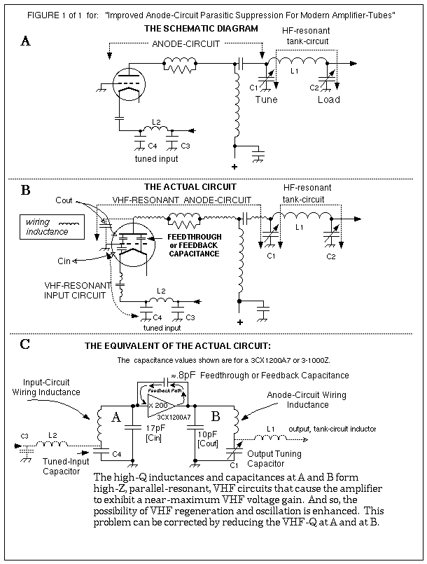
This is the unedited version of the article "Improved Anode-Circuit Parasitic-Suppression For Modern Amplifier-Tubes," which was published on page 36 of the October 1988 issue of QST. A subsequent discussion on this topic appeared in the September and October...
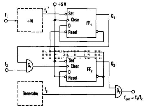
This circuit generates an output frequency that is linearly proportional to the ratio of two input frequencies. Each pulse of the bias frequency will open a switch for a period equal to half of the second input frequency, allowing...
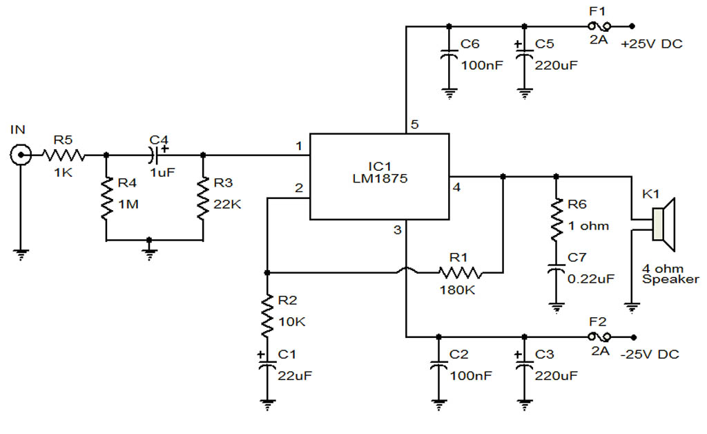
The circuit illustrates a 20-Watt audio amplifier diagram based on the LM1875 integrated circuit (IC). It is designed for use in automotive applications and provides an output power of 20 Watts. The 20-Watt audio amplifier circuit utilizing the LM1875 IC...
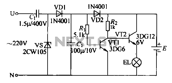
An automatic emergency lighting circuit is presented, suitable for self-installation in households. It utilizes smaller components, resulting in a lower cost. Under normal conditions, the 220V AC mains voltage is reduced by capacitor C1, and then processed through a...
More: An electronic schematic is a representation of the components and connections within an electronic circuit. It serves as a blueprint for constructing electronic devices, allowing engineers and technicians to visualize how components interact and function together. The schematic...