
Low-Drift/Low-Noise Dc Amplifier

The described circuit employs a low-noise operational amplifier (IC1) that operates in a chopper-stabilized configuration. This design is particularly advantageous for applications requiring high precision and stability over varying temperatures. The low offset voltage and minimal drift characteristics make this amplifier suitable for sensitive measurement tasks. The noise performance, specified at less than 40 nV within a 10-Hz bandwidth, indicates that the circuit is designed to minimize interference from external noise sources, which is critical for high-fidelity signal processing.
The 74C04 inverters are utilized to generate a stable 2-phase square-wave clock signal, essential for the chopper modulation technique. This clock signal, operating at approximately 350 Hz, is responsible for switching the input signal on and off, effectively reducing low-frequency noise and drift. The synchronous operation of switches S1 and S2 ensures that the input signal is accurately sampled and processed.
The demodulation stage, comprising switches S3 and S4, is crucial for retrieving the amplified signal from the chopper-modulated output of IC1. This stage ensures that the output retains the correct amplitude and polarity, which is necessary for the subsequent DC amplification by IC2. The integration of the square-wave signal into a DC output is achieved through the output stage, which effectively converts the modulated signal back into a usable form.
Feedback resistors R1 and R2 play a vital role in determining the gain of the amplifier circuit. By setting the ratio of these resistors, the gain can be precisely adjusted to the desired level, in this case, a gain of 1000. This feedback mechanism not only stabilizes the circuit but also allows for fine-tuning of the output voltage, ensuring that it meets the requirements of the specific application. Overall, this circuit design exemplifies advanced techniques in analog signal processing, yielding a high-performance amplifier suitable for demanding electronic applications. Figure 39-2"s circuit combines a low-noise op amp, IC1, with a chopper-based carrier-modulation scheme to achieve a low-noise, low-drift dc amplifier whose performance exceeds any currently available monolithic amplifier. The amplifier"s offset is less than 1, and its drift is less than 0.05 /iV/°C. This circuit has noise within a 10-Hz bandwidth less than 40 nV. The amplifier"s bias current, which is set by the bipolar input of IC1, is about 25 nA. The 74C04 inverters (IC3 to IC6) form a simple 2-phase square-wave clock that runs at about 350 Hz. The complementary oscillator signals ( and O2) provide drive to SI and S2, respectively, causing a chopped version of the input to appear at ICl"s input.
IC1 amplifies this ac signal. S3 and S4 synchronously demodulate ICl"s square-wave output. Because S3 and S4 switch synchronously with SI and S2, the circuit presents proper amplitude and polarity information to IC2, the dc output amplifier. This output stage integrates the square wave to provide a dc voltage output. Rl and R2 divide the output and feed it back to the input chopper where the divided output serves as a zero signal reference.
The ratio of Rl and R2 sets the gain, in this case to 1000.
Related Circuits
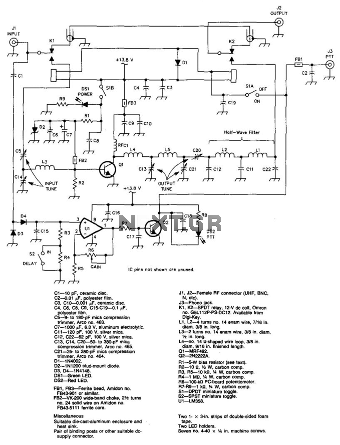
A 100 W output at 50 MHz is available from this circuit. U1 and Q2 form a T-R relay driver, switching the amplifier on when RF input at J1 is sensed. During receive periods, J1 and J2 are directly...
This design circuit outlines a simple, low-cost, and ultra-compact VHF/UHF Low-Noise Amplifier (LNA) that can be implemented using the MAX2664 and MAX2665 devices, which are specifically tailored for VHF/UHF applications. The MAX2664 operates within the UHF frequency range of...
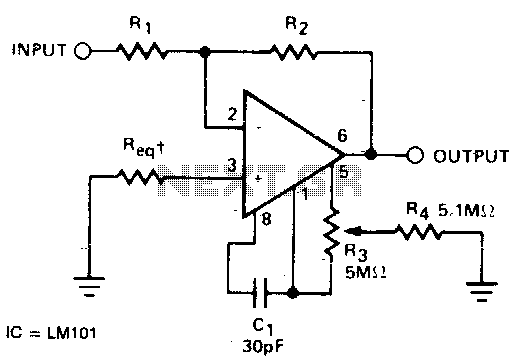
The required resistance (Req) may be zero or equal to the parallel combination of resistors R1 and R2 to achieve minimum offset. The circuit configuration described involves the use of two resistors, R1 and R2, connected in parallel. In a...

22W into 4 Ohm power amplifier, Variable Low Pass Frequency: 70-150Hz. This unit is intended to be connected to an existing car stereo amplifier, adding functionality. The described power amplifier is designed to deliver an output power of 22 watts...
This amplifier is designed to amplify RF signals from an antenna by 10 dB and operates as a Class A amplifier using the BFQ34 transistor from Philips. The BFQ34 is packaged in an SOT122A case. The BFQ34T variant is...

This stereo amplifier utilizes the NE5517/A and features an excellent tracking accuracy of 0.3 dB, which is typical. The offset can be adjusted using the potentiometer, Rp. For AC-coupled amplifiers, the potentiometer can be substituted with two 5.1 k...