
Baby Monitor Circuit
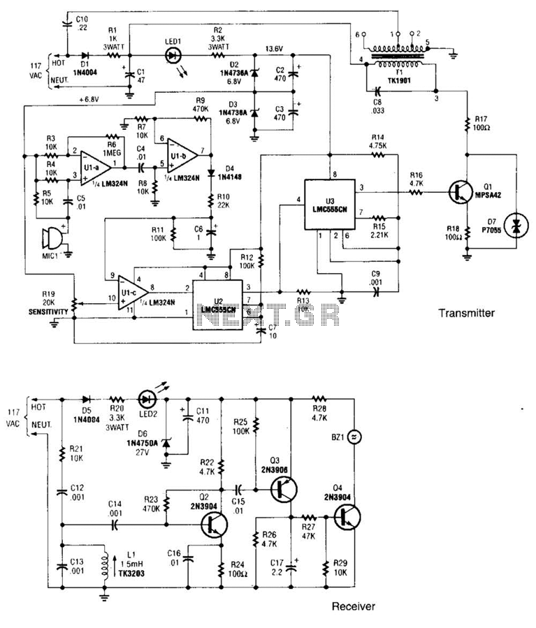
An electret microphone element (MIC1) is used for sound pickup. The microphone's output is AC-coupled through capacitor C5 to operational amplifier U1-a (configured as a non-inverting amplifier with a gain of about 100). The output from U1-a at pin 1 is then AC-coupled through capacitor C4 to the non-inverting input of U1-b (which provides an additional gain of 48) at pin 5. The output of U1-b at pin 7 is routed through diode D4 and resistor R10, and then across resistor R11 and capacitor C6 to the inverting input of U1-c, which is biased to a positive voltage set by the sensitivity control resistor R19. This bias voltage establishes a threshold at which the output of U1-c switches from high to low. During standby, the output of U1-c at pin 8 is held at about 12V when the voltage developed across capacitor C6 is below the bias voltage at pin 10. When a sound of sufficient intensity and duration is detected, the voltage at pin 9 of U1-c exceeds the threshold set by R19, causing the output at pin 8 to transition low. This low signal is sent to pin 2 of U2 (a 555 timer configured as a monostable multivibrator). The output of U2 is driven high for approximately one second, determined by the time constant of resistor R12 and capacitor C7. The output at pin 3 of U2 is applied to pin 4 of U3 (a second 555 timer configured for astable operation with a frequency of about 125 kHz). This configuration causes U3 to oscillate, producing a near square-wave output that drives Q1 into conduction. The output of Q1 is connected to a parallel-tuned circuit formed by the primary of transformer T1 and capacitor C8. This tuned circuit reshapes the 125 kHz signal, generating a sine-wave-like output across both the primary and secondary of T1. The signal at T1's secondary, approximately 1 or 2V peak-to-peak, is impressed across the AC power line and distributed throughout the building without interfering with other electrical appliances connected to the line. A transient suppressor diode D7 is included to protect Q1 from voltage spikes that may appear across the power line and couple into the circuit via T1.
In the receiver section, power is also derived from the AC line through a traditional half-wave rectifier (D5). The resulting DC voltage is regulated to 27V by diode D6 and resistor R20, then filtered by capacitor C11 to provide a clean DC power source for the circuit. A light-emitting diode, LED2, connected in series with R20, indicates visually that the circuit is powered and ready to receive signals. The 125 kHz signal is extracted from the AC line and coupled through resistor R21 and capacitor C12 to a parallel-tuned local oscillator (LO) circuit consisting of capacitor C13 and inductor L1, which passes the 125 kHz signals while attenuating others. The 125 kHz signal is then fed through capacitor C14 to the base of transistor Q2, which is configured as a high-gain linear amplifier, thereby boosting the low amplitude of the 125 kHz signal. The RF output of Q2 is AC-coupled to the base of Q3 through capacitor C15. Transistor Q3 functions as both an amplifier and a detector. Without a bias voltage at its base, Q3 remains off until driven by the amplified 125 kHz signal. When forward-biased, the collector voltage of Q3 rises. Capacitor C16, connected across Q3's collector resistor, filters the 125 kHz signal, resulting in a DC voltage. As the collector voltage of Q3 increases, it drives transistor Q4 into conduction, allowing current to flow into piezo buzzer BZ1, producing an audible tone to alert individuals nearby that attention is needed. Transmitter operation. Operating power for the transmitter circuit is derived directly from the ac line. The dc power to operate the circuit is generated in two stages, one for an RF power-am-plifier stage, and the second for the remainder of the circuit. The ac line voltage is applied to Dl, which half-wave rectifies the ac input. The resulting dc voltage (approximately 30V under load) is fed across an RC filter (comprised of Rl and 01) and used to operate amplifier, Ql.
The second stage of the power supply (composed of LED1, R2, D2, D3, 02, and 03, which forms a regulated +13.6-V, center-tapped supply) feeds the remainder of the circuit. LED1 is connected in series with R2 and is used as a visual power-on indicator for the transmitter. An electret microphone element (MIC1) is used as the pick-up. The output of the microphone is ac coupled through 05 to Ul-a (a noninverting op amp with a gain of about 100). The output of Ul-a at pin 1 is ac coupled through 04 to the noninverting input of Ul-b (which provides an additional gain of 48) at pin 5.
The output of Ul-b at pin 7 is then fed through D4 and RIO, and across Rll and 06 to the inverting input of Ul-c which is biased to a positive voltage that is set by SENSITIVITY-Control R19. This represents a threshold voltage at which the output of Ul-c switches from high to low. During standby, the output of Ul-c at pin 8 is held at about 12 V when the voltage developed across 06 is less than the bias-voltage setting at pin 10.
When a sound of sufficient intensity and duration is detected, the voltage at pin 9 of Ul-c exceeds the threshold level (set by R19), causing Ul-c`s output at pin 8 at go low. That low is applied to pin 2 of U2 (a 555 oscillator/timer configured as a monostable multivibrator).
This causes the output of U2 to-go high for about one second, as determined by the time constant of R12 and 07. The output of U2 at pin 3 is applied to pin 4 of IJ3 (a second 555 oscillator/timer that is configured for astable operation, with a frequency of about 125 kHz).
That causes U3 to oscillate, producing a near square-wave output that is used to drive Ql into conduction. The output of Ql is applied across a parallel-tuned circuit composed a Tl`s primary and 08. The tuned circuit, in turn, reshapes the 125-kHz signal, causing a sine-wave-like signal to appear across both the primary and the secondary of Tl.
The signal appearing at Tl`s secondary (about 1 or 2 V peak-to-peak) is impressed across the ac power line, and is then distributed throughout the building without affecting other electrical appliances connected to the line. Transient suppressor D7 is included in the circuit to help protect Ql from voltage spikes that might appear across the power line and be coupled to the circuit through Tl.
Receiver operation. Power for the receiver, as with the transmitter, is derived from a traditional half-wave rectifier (D5). The resulting dc voltage is regulated to 27 V by D6 and R20, and is then filtered by Oil to provide a relatively clean, dc power source for the circuit.
A light- emitting diode, LED2, connected in series with R20 provides a visual indication that the circuit is powered and ready to receive a signal. The 125-kHz signal is plucked from the ac line and coupled through R21 and 012 to a parallel-tuned LO circuit, consisting of 013 and LI.
That LC circuit passes 125-kHz signals while attenuating all others. The 125-kHz signal is fed through 014 to the base of Q2 (which is configured as a high-gain linear amplifier), which boosts the relatively low amplitude of the 125-kHz signal. The RF output of Q2 is ac coupled to the base of Q3 through 015. Transistor Q3 acts as both an amplifier and detector. Because there is no bias voltage applied to the base of Q3, it remains cut off until driven by the amplified 125-kHz signal.
When Q3 is forward biased, its collector voltage rises. Capacitor 016, connected across Q3`s collector resistor, filters the 125-kHz signal so that it is essentially dc. When the voltage at the collector of Q3 rises, Q4 is driven into conduction. That causes current to flow into piezo buzzer BZ1, producing a distinctive audio tone that alerts anyone within earshot that the baby needs attention.
🔗 External reference
Related Circuits
The primary components of this doorbell circuit include two NE555 timer integrated circuits (ICs). When the switch S1 is pressed momentarily, the loudspeaker emits a bell tone for the duration determined by the time period of the monostable multivibrator...

This simple circuit is designed to check transistors, allowing measurements down to 40 ohms across the collector-base or base-emitter junctions. It is also capable of testing output power transistors in amplifier circuits. The circuit operates with a 555 timer...

The circuit requires a 15-volt power supply and employs a precision operational amplifier, CA3193 BiMOS, to amplify the generated signal by more than 500 times. Three 22-megohm resistors are utilized to ensure a large-scale output in the event of...
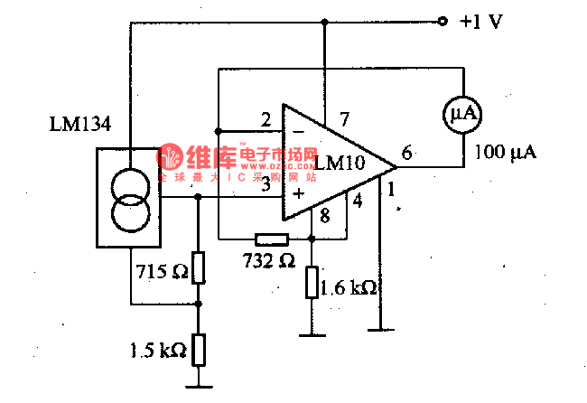
This is an electric thermometer circuit composed of the LM134. In the circuit, the voltage or current output by the LM134 is proportional to the thermodynamic temperature, which can be read on a 100 µA meter. The test temperature...

Rechargeable ago memory circuit. Before the memory circuit is activated, a delay reset circuit is utilized. When the input signal triggers an action, timing begins, and after a specified delay, the circuit reverts to its original state. During this...

The hobby circuit described utilizes a unique approach to generate approximately 12,000 volts with a current of about 5 µA. It employs two silicon-controlled rectifiers (SCRs) that form dual pulse generator circuits. These SCRs discharge a 0.047 µF capacitor...
Warning: include(partials/cookie-banner.php): Failed to open stream: Permission denied in /var/www/html/nextgr/view-circuit.php on line 713
Warning: include(): Failed opening 'partials/cookie-banner.php' for inclusion (include_path='.:/usr/share/php') in /var/www/html/nextgr/view-circuit.php on line 713