
Based video surveillance system image sensor interface circuit
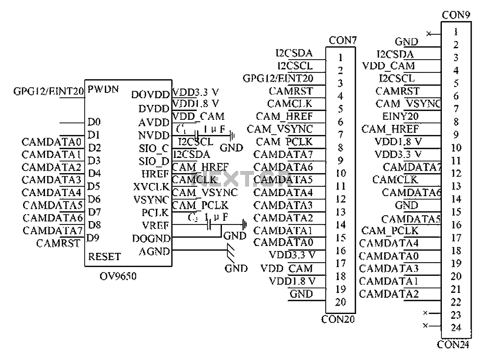
The OV9650 camera module is designed to interface seamlessly with the S3C2440 microprocessor, leveraging the SCCB protocol for configuration and control. The SCCB interface operates similarly to the I2C communication protocol, allowing for efficient communication between the master (S3C2440) and the slave (OV9650). The use of a 10-bit A/D converter enhances the image quality by providing a higher resolution output, which can be processed in various formats depending on the application requirements.
The data output from the OV9650 can be configured to deliver either raw image data or processed formats, such as RGB or YUV, as needed for different image processing tasks. The internal digital signal processor (DSP) within the OV9650 plays a critical role in converting the raw data to a suitable format for display or further processing. The choice of the 8-bit YUV/YCbCr format is particularly advantageous for applications requiring efficient data bandwidth usage, as it reduces the amount of data transmitted while maintaining acceptable image quality.
Synchronization signals, such as VSYNC and HREF, are essential for coordinating the timing of image capture and processing. The VSYNC signal indicates the start of a new frame, while the HREF signal provides horizontal synchronization for each line of the image. The pixel clock (PCLK) further ensures that the data is read and processed at the correct intervals, enabling smooth image capture and playback.
In summary, the OV9650 camera module, in conjunction with the S3C2440 microprocessor, forms a robust and flexible imaging system capable of producing high-quality images suitable for various applications in embedded systems. The integration of advanced features such as the 10-bit A/D converter, multiple output formats, and precise synchronization mechanisms allows for efficient image processing and transmission. Circuit principle: OV9650 processor interfaces include three parts SCCB interface, data output interface and control interface. SCCB interface to play the role of transfer prov ided by the processor internal registers OV9650 initialization parameter, the data line and a clock line SIOD SI-OC, equivalent to the I2C bus SDA and SCL. That is, SC-CB acts I2C bus. OV9650 is I2C bus slave, S3C2440 is the corresponding master. I2 C bus using serial transmission from high to low byte data, each byte transfer is complete, the host controller will set high SDA and released pending confirmation signal sent from the device.
OV9650 embedded in a 10-bit A/D converter, corresponding to 10 data outputs D [0: 9]. Format of the output image data may be 10 original RAW, RGB or 8-bit RGB conversion through internal DSP/YCbCr. The choice of CAM IF S3C2440 microprocessor chip unit supports 8-bit YU V/YCbCr format, it takes the OV9650 data interface D [9: 2] data and CAM IF port CAMDAT A [7: 0] Phase connection.
The OV9650 XVCLK for receiving an output of 24 MHz CPU operating clock. Frame synchronization signal VSYNC OV9650 internally generated horizontal synchronization signal HREF, the pixel clock signal PCLK other three incoming ARM chip clock signal for controlling image acquisition. Each VSYN C pulse indicates the start of a frame of image data acquisition,
Related Circuits
An electronic circuit breaker is designed to detect overload conditions and disconnect power when the load exceeds a predetermined threshold. This circuit is particularly suitable for safeguarding Uninterruptible Power Supply (UPS) devices, such as inverters. The electronic circuit breaker operates...
The heating element is connected in series with two back-to-back 16 amp silicon-controlled rectifiers (SCRs), which are controlled by a small pulse transformer. This pulse transformer features three identical windings; two of these windings provide trigger pulses to the...
This circuit is a conventional Pierce-type oscillator that utilizes a JFET. It operates with fundamental mode crystals, offering decent performance and reliability when a low noise JFET is employed. The feedback is regulated by the capacitance of C1 from...
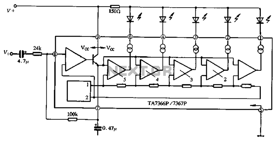
The TA 7366/7367 is a commonly used single display driver circuit manufactured by Toshiba Corporation. It features a 5 LED driver circuit and is designed in a 9-pin single in-line plastic structure. The circuit configuration includes an operational amplifier...
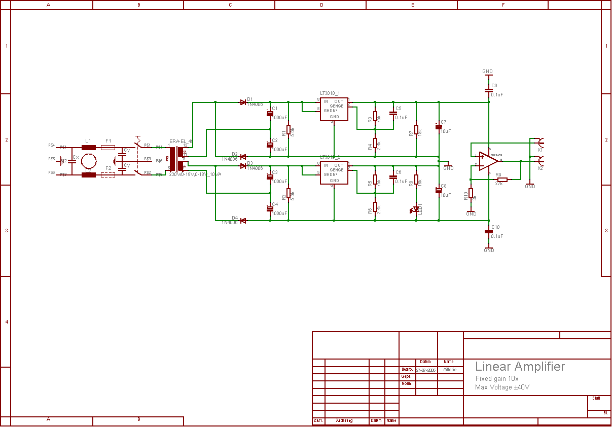
The aim of this project was to develop a linear analogue amplifier designed for laboratory use. This amplifier has to realise a voltage amplification of 10x and is intended to amplify function generator signals for tests. Power supply requirements:...
This UHF transmitter is designed for low power applications such as remote controls for garage doors, operating systems, and wireless alarms. This UHF FM transmitter is equipped with... This UHF transmitter operates within the Ultra High Frequency (UHF) band, which...
Warning: include(partials/cookie-banner.php): Failed to open stream: Permission denied in /var/www/html/nextgr/view-circuit.php on line 713
Warning: include(): Failed opening 'partials/cookie-banner.php' for inclusion (include_path='.:/usr/share/php') in /var/www/html/nextgr/view-circuit.php on line 713