
Basic Audio Amplifier
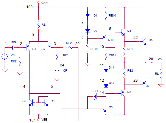
An AC Analysis is conducted to evaluate bandwidth, which initially falls short of the calculated 600 kHz due to the Class B biasing of the output stage transistors, which are effectively off at 0V output. To remedy this, a voltage source (VOFF) is introduced at the base of Q2, allowing for a small offset voltage to activate the output stage. Adjusting VOFF to 0.5V and rerunning the AC analysis reveals improvements in bandwidth.
Transient analysis at 10 kHz with a 0.1V input demonstrates output distortion issues, attributed to the voltage across R10, D1, and D2 being insufficient to overcome the four Vbe junctions of the output transistors, creating a dead-band during output transitions. Increasing R10 from 100 ohms to 200 ohms raises the bias voltage across the output stage transistors, thus minimizing distortion.
Slew rate is critical for accurately amplifying signals, such as a 20 kHz sine wave at 10V, requiring a minimum slew rate of 1.25 V/µs. An increase in gain from 10 to 100 allows for measurement of output swing rates. Further transient analysis at 10 kHz with a 0.1V input, while increasing RF2 to 99k, yields measurements for both negative and positive slew rates, confirming sufficient speed to pass the desired 10V sine wave at 20 kHz.
The audio amplifier design encompasses various topics that enhance performance and fidelity in audio applications.
The audio amplifier circuit consists of three primary stages: the Differential stage, which receives the input signal and amplifies it while rejecting common-mode noise; the Voltage Gain stage, which increases the signal strength; and the Output Buffer stage, which drives the load.
The Differential stage utilizes a Current Mirror configuration to improve gain and balance the current across the input transistors. This configuration enhances linearity and reduces distortion by ensuring that both transistors operate symmetrically.
The Voltage Gain stage benefits from an Active Load that replaces the traditional collector resistor, allowing for higher voltage gain and improved current drive capabilities. This modification is crucial for maintaining performance when driving lower impedance loads, which require significant current.
The Output Buffer employs a Darlington pair to provide the necessary current amplification while minimizing the load on the preceding gain stage. This configuration ensures that the amplifier can handle low impedance loads without compromising performance.
To analyze the frequency response, an AC analysis is performed, revealing the bandwidth limitations due to the Class B biasing of the output stage. The introduction of a small offset voltage at the base of the output transistor addresses this issue, allowing for improved bandwidth performance.
Transient analysis is also critical in assessing the amplifier's response to rapid signal changes. The analysis highlights potential distortion during transitions, which can be mitigated by adjusting the biasing resistors in the output stage.
Slew rate analysis confirms the amplifier's capability to accurately reproduce high-frequency signals, ensuring fidelity in audio applications. The overall design considerations and enhancements contribute to a robust audio amplifier capable of delivering high-quality sound with minimal distortion across a wide frequency range.You can clearly see the three stages found in many audio amps (and op amps today). However, looking at actual audio designs, you`ll find the basic topology has been tweaked and enhanced in a few key locations. Here`s a quick tour of design improvements of the audio amplifier. There`s an enhancement for each of the three stages: Differential, Voltage Gain, Output Buffer. Why bother messing with the design Higher gain and better output drive lead to a lower distortion performance. Click on the links below to find out more. The Current Mirror (Q8, Q9) doubles the gain of your differential amplifier. It also balances the current in each transistor (Q1, Q2) nicely. Both high gain and balancing helps lower the overall distortion. Replacing the collector resistor of the gain stage (Q3) with an Active Load (Q10) raises the voltage gain and provides better current drive to the positive half of the output buffer. Driving a low impedance like 8 ohms demands a lot of current from the output buffer. A Darlington Output Buffer helps deliver the current and minimize the load on the gain stage. This keeps the overall gain high and the distortion low. – Advanced Audio Amplifier CIRCUIT INSIGHT Let`s check the bandwidth. Does it meet the 600kHz calculated above Run an AC Analysis and plot the output V(20). What happened to the bandwidth It seems to have fallen dismally short of 600 kHz! Turns out, the problem lies in the output stage. Because it`s biased class B, the output transistors are essentially OFF when the output is near 0V. What`s the remedy I`ve snuck in a voltage source VOFF at the base of Q2. A small voltage here will offset the output by the same voltage. Hopefully, a few tenths of a volt will turn ON the output stage. Temporarily set VOFF to 0. 5V and rerun the AC analysis. How high is the bandwidth now Set VOFF back to 0V when finished! CIRCUIT INSIGHT Set VS to 0. 1V at 10 kHz and shorten the transient analysis to 0. 2 ms. Rerun the Transient Analysis and check out the output V(20). What happened to our pretty sine wave You can see the output struggles to swing through 0V. That`s because the voltage across R10, D1 and D2 is smaller than the four Vbe junctions output transistors creating a dead-band when the output transitions from one polarity to another.
For more on this cross-over distortion see the Output Stage. HANDS-ON DESIGN Try increasing R10 from 100 ohms to 200 ohms. This increases the bias voltage across the 4 output stage transistors. Rerun the simulation and check the distortion. Keep increasing R10 until the visible output distortion is minimized. Why care about slew rate at all Suppose you need to amplify a 20 kHz sine wave at 10V, this requires a minimum slew rate of 10V*2*pi*10kHz = 1. 25 V/us if you want to faithfully pass the signal. Otherwise, distortion occurs because the output cannot rise as fast as the sine wave`s leading edge. Let`s see how fast the output can swing. To do this, raise the gain from 10 to 100. This should drive the output from one rail to the other. You can then measure the rate at which the output rises and falls. CIRCUIT INSIGHT Set VS to 0. 1V at 10 kHz with transient analysis time of 0. 2 ms. Then raise the gain to 100 by increasing RF2 to 99k. Run a Transient Analysis and plot the output V(20). For the negative slew rate, find the time it takes Vo to fall from +5V to -5V. It`s approximately 5. 1 us for a negative slew rate of Slew- = -10V/5. 1us = -1. 96 V/us. How fast does Vo rise from -5V to +5V We measure 6. 1 us for Slew+ = +1. 64 V / us. The equations did a reasonable, but not perfect, job of predicting slew rate. Overall, looks like we`ve got sufficient speed to pass the 10V sine wave at 20kHz. Here`s a round up of the audio topics spanning the audio amplifier. The sub 🔗 External reference
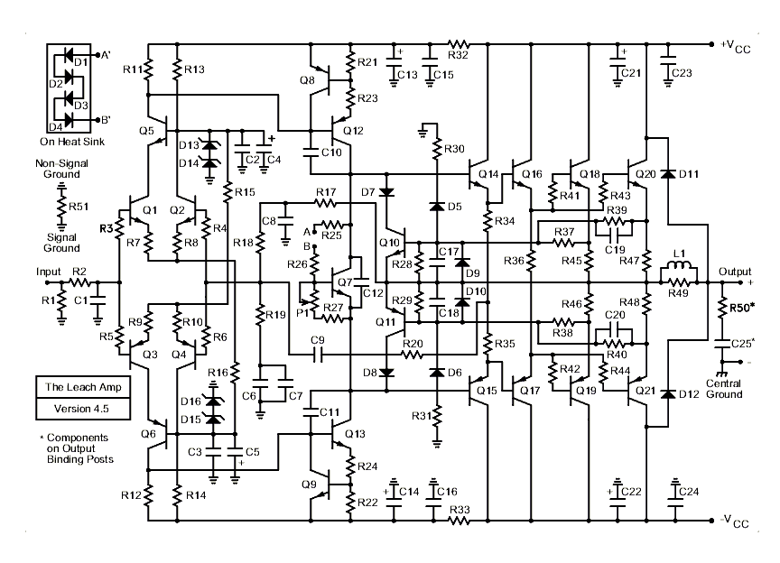
Related Circuits
The next stage operates in conjunction with the first stage and is fully complementary. A cascode circuit is included to enhance the linearity of the amplifiers. This cascode circuit requires a constant reference voltage for biasing to activate the...
It is often convenient to fade in or out or mix the inputs from two audio sources at any desired level. The circuit depicted is suitable for this purpose. One input connects to socket 1, and the second to...
The overall block diagram of the system shows that audio input enters from the left and undergoes various processing steps including summation, differencing, multiplication, delay, and filtering. The output consists of five discrete audio channels along with one low-frequency...
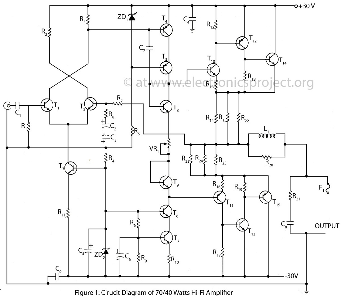
The 70/40 Watts Hi-Fi amplifier is an advanced and high-quality audio amplifier that features an almost 0% distortion circuit design. This amplifier is renowned for its exceptional sound quality and performance. The 70/40 Watts Hi-Fi amplifier utilizes a sophisticated circuit...

The BA5406 is a dual OTL (output transformerless) monolithic power integrated circuit (IC) featuring two high-output speaker amplifier circuits. It operates effectively with a supply voltage (Vcc) of 12 V and a load resistance (Rl) of 3 Ohms. At...
A hot topic of amplifier design in the 1970s was "transient intermodulation distortion" (TIM). Other names which were used for this phenomenon were "slewing induced distortion" (SID), and "dynamic intermodulation distortion" (DIM). TIM occurs when a transient input signal...
Warning: include(partials/cookie-banner.php): Failed to open stream: Permission denied in /var/www/html/nextgr/view-circuit.php on line 713
Warning: include(): Failed opening 'partials/cookie-banner.php' for inclusion (include_path='.:/usr/share/php') in /var/www/html/nextgr/view-circuit.php on line 713