
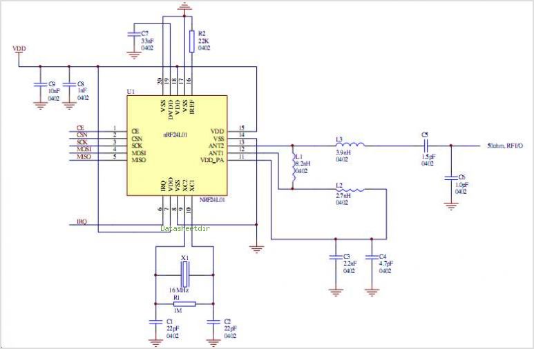
Basic circuit diagram of a 2.4 GHz radio system-on-chip CC2430
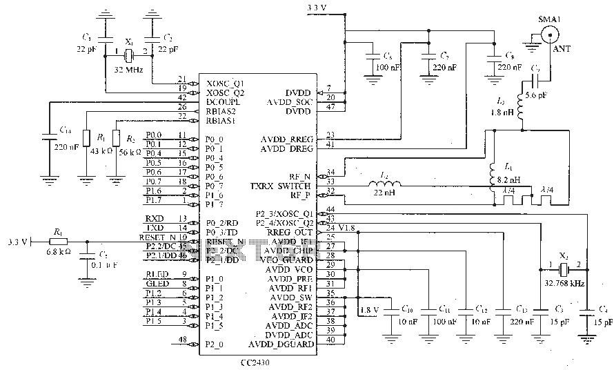
The schematic includes various capacitors and inductors that play critical roles in the performance of the oscillator circuits and overall system stability. The 22 pF capacitors at the 32 MHz oscillator ensure that the frequency remains stable and accurate for standard operations, which is essential for timing applications. The 15 pF capacitors connected to the 32.768 kHz oscillator are particularly important for low-power modes, allowing the device to conserve energy while maintaining functionality during sleep states.
Noise reduction is a significant consideration in this design, as evidenced by the use of multiple capacitors for filtering. Capacitors C5, C6, C7, and C8 filter out high-frequency noise that could disrupt the microcontroller's operation, while C9's role in the unbalanced transformer circuit is crucial for impedance matching, ensuring efficient signal transmission and reception in RF applications.
The inductors L1, L2, and L3 are carefully chosen to match the required inductance values for the circuit, optimizing the performance of the microwave transmission line. The values of these inductors indicate a design that is tuned for specific RF characteristics, which is vital for maintaining signal integrity.
Decoupling capacitors C10 to C14 are strategically placed to stabilize the power supply, mitigating voltage fluctuations that could affect the microcontroller's performance. The bias resistors R1 and R2 are selected to provide the necessary bias current, ensuring that the oscillators operate within their intended specifications.
Overall, this circuit design exemplifies a comprehensive approach to oscillator circuit design, focusing on stability, efficiency, and noise reduction, which are critical for modern electronic applications. The choice of components and their configurations reflect an understanding of RF principles and low-power design strategies, making this circuit suitable for various applications requiring reliable timing and communication capabilities.Figure C1, C2 is 22pF capacitor connected to 32 MHz .png">crystal oscillator circuit , the use of quartz crystal oscillator for normal operation. C3, C4 is 15 pF capacitor connected to the 32.768 kHz crystal oscillator circuit, quartz crystal for this work in sleep mode, reducing power consumption. C5 = 0.1 F, for removing some of the clutter, to prevent the microcontroller error reset. C6 ~ C8 were 100 nF, 220n F, 220 nF, used as a filter to remove clutter to make a more stable voltage.
C9 = 5.6 pF, Unbalanced transformer circuit by the capacitor C9 and inductor L1, L2, L3 and microwave transmission line consisting of a PCB, the entire structure to meet the RF input / output matching resistor (50 ) requirements, L1, L2, L3, respectively 8.2 nH, 22 nH, 1.8 nH. C10, C11, C12, C13, C14 as decoupling capacitors for power supply filtering, to improve the stability of the work of the chip.
Bias resistor R1, R2 respectively 43 k , 56 k , R1 is used to set the 32 MHz crystal oscillator precision bias current. Since the CC2430 chip has low power consumption, use 2 2 800 mAh of battery power the node. External antenna antenna choice.
Related Circuits
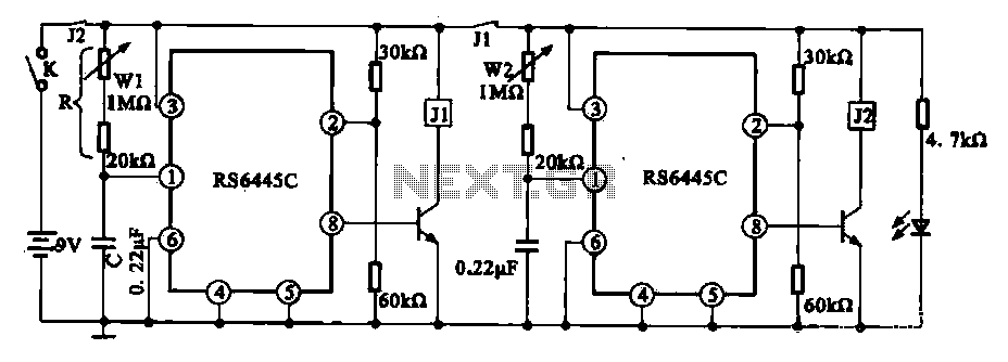
The timing integrated circuit (IC) RS6445C functions as a blocking oscillator. It features two segments, WI and W2, which are utilized to adjust the working time and the closure time. These adjustments can be continuously set within a range...
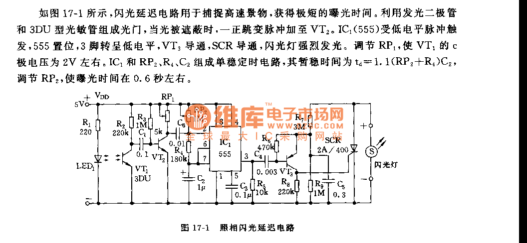
As shown in figure 17-1, the camera flash delay circuit is designed to capture high-speed scenes, allowing for very short exposure times. The light gate consists of a luminous diode and a 3DU type photosensitive tube. When the light...
Do you have disco ears? If people ask you this and you are still well below 80, you may be experiencing hearing loss, which can result from prolonged exposure to loud music. The severity of the issue may not...
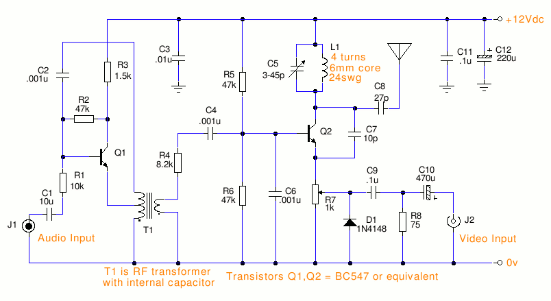
This is a small TV transmitter circuit that transmits in VHF, utilizing negative sound modulation and PAL video modulation. It is suitable for countries that use the B and G system. T1 refers to a type of transformer. The...
The NRF24L01 is a single-chip radio transceiver designed for operation within the 2.4 to 2.5 GHz ISM band. The NRF24L01 transceiver is a highly integrated solution that facilitates wireless communication in the 2.4 GHz ISM band, making it suitable for...
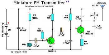
This small FM band transmitter utilizes only two 2N2222 transistors and is capable of transmitting signals up to 1 kilometer away, provided there are no obstacles between the two antennas. The circuit features a microphone preamplifier stage with the...