
555 camera flash delay circuit
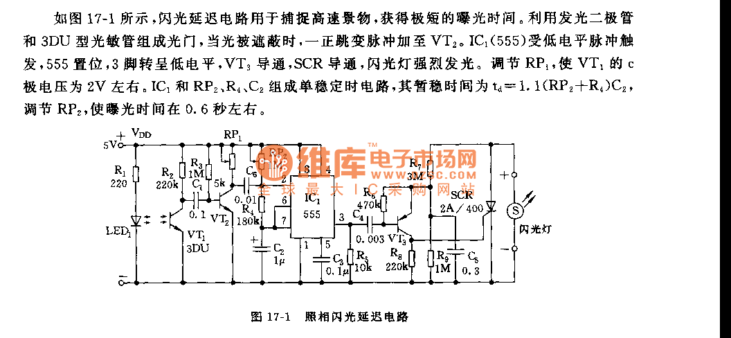
The camera flash delay circuit utilizes a light gate mechanism to accurately time the activation of the camera flash during rapid events. The luminous diode emits light that is detected by the 3DU photosensitive tube. In normal conditions, the photosensitive tube remains conductive, allowing current to flow through the circuit. However, when an object passes through the light beam, it casts a shadow on the photosensitive tube, leading to a sudden change in its conductivity.
This change generates a positive transition pulse that is sent to a transistor (VT2), which acts as a switching element in the circuit. The pulse triggers the 555 timer IC (IC1), configured in a monostable mode. Upon receiving the low-level pulse, the 555 timer initiates a timing cycle, which determines the duration of the flash. The output pulse from the 555 timer controls the flash mechanism, ensuring that the flash is activated for a very short duration, suitable for freezing motion in high-speed photography.
The circuit may also include additional components such as resistors and capacitors to fine-tune the timing characteristics and ensure proper operation of the 555 timer. The design allows for adjustments to be made, enabling the user to optimize the exposure time based on specific lighting conditions and the speed of the subject being photographed. Overall, this camera flash delay circuit is an effective solution for capturing fleeting moments with precision and clarity.As the figure 17-1 showns, the camera flash delay circuit can be used to capture the high-speed scene, and you can get a very short exposure time. The light door is composed of the luminous diode and the 3DU type photosensitive tube. When the light is shadowed, the positive transition pulse adds to the VT2. The IC1(555) is triggered by the low-level pulse, 5.. 🔗 External reference
Related Circuits

This device prevents paper notes and memos from being overlooked. A paper note placed between two fingers made of a conducting material (metal or conductive plastic) breaks the circuit, allowing pair 1 of Ul-a to go high. This causes...
This type of sensor switch is ideal for creating touch-operated bells and buzzers in small toys, which function for a limited duration before automatically shutting off. The trigger's input impedance is very high, allowing the touch sensor switch to...

An AC mains operated single LED flasher circuit is designed using the widely used CMOS timer chip TLC555. The entire circuit is powered directly by the grid supply of 230VAC through a capacitive potential divider and associated components. This LED...

The computer control system is designed to detect signal path switching, requiring multiple input interface expansions. This system can switch all signal inputs into the computer. By utilizing a programmable chip, the 8255 expansion input interface allows for three...

An automatic cycle switch circuit utilizing a 555 integrated circuit (IC) as the control element. It incorporates a capacitive step-down circuit and employs a bidirectional thyristor to control relays or loads with specific on and off timing. The circuit...

This project involves a straightforward soil moisture detection circuit that utilizes only four components and operates with a 3-volt battery. The circuit is designed to identify the presence of moisture in the soil of any plant and activate an...