
Bicycle alarm electronic project

The circuit design incorporates a series of logic gates and components to create a functional alarm system. The use of a NOR gate as a core component allows for the implementation of both the alarm setting mechanism and the LED alert system. The transistor switch plays a critical role in controlling the power supply to the alarm system, ensuring that the alarm can be reset effectively. The keypad interface simplifies user interaction, while the choice of components balances functionality with cost-effectiveness. The flashing LED serves both as a deterrent and as an indicator of the alarm's status, enhancing the overall effectiveness of the security system. The design reflects a thoughtful consideration of user needs and technological constraints of the time, demonstrating an understanding of fundamental electronics principles.This is a project that I undertook during June 1996 as my final year electronics project. The entire circuit was built using individual components including logic gate ICs and and keyboard decoder IC. Since them electronics has moved on and if this was created today most of the functionality would instead be implemented using a microprocessor / mi
crcontroller such as the Arduino prototyping board. This is however an example of how circuits can be designed using logic components. To set the alarm the supply must be disconnected. To achieve this a transistor switch is used to disconnect the supply when the full or part set switch is pressed. This is achieved using a NOR gate (IC2D). This is a 18 pin IC which uses a matrix output type keypad. The PIN number can be separately programmed directly from the keypad. This makes programming much easier. The pin layout is shown below. The IC is CMOS compatible and has a key-in echo, which bleeps every time a key is pressed. The following circuit would have to be fairly complex to use this IC. Below is the circuit diagram if the IC was for use as a door opener. The choice of the decoder was based on two main factors. The first was the required complexity of the following circuit. As the RS7225 gave fixed output levels the IC could drive combination logic directly whereas the UA3730 would require special sequential logic to decode the outputs.
The second factor was cost. The cost of the two ICs is very much the same but the cost of the required keypad was much cheaper for the telephone type keypad. Also a membrane keypad was available for the telephone type which gave a level of waterproofing. As the RS7225 required the disconnection of the supply to reset the outputs a transistor switch has been used to disconnect the supply and reset the alarm.
This is triggered by IC2D which is connected to the part set and the full set selections which switches TR1. The alarm set indicator is taken from pin 8 on IC1. As a warning to potential thiefs the LED was to flash on and off at a constant speed. This alerts the thief better than a constant light as a flashing light is much more obvious and more noticeable.
This could be achieved by using 2 methods, a 555 counter or a different astable firing a transistor hence switching the LED on and off. The enable input would come from pin 8 on IC1 which would switch the astable on and off. When in the off state then the current consumed would be very low. When in the flashing state the current consumption would still be lower than the 555s. The frequency is equal to the multiple of the capacitance and the resistance. This circuit only requires ½ a (Quad 2 input) NOR IC, 1 resistor, 1 capacitor, and 1 transistor (the other resistor is for current limiting the LED and would be required anyway.
It is very important that the NOR gates have buffered outputs, but most CMOS ICs are buffered anyway and so this is not a deciding factor. The time constant used is a 0. 3 seconds giving a frequency of about 3 Hz. This is slow enough to be seen but fast enough so as it can be seen within a short time period. This time constant was given by using a 100nF capacitor and a 3. 3M resistor. These were the nearest standard values. This gave a reasonable flashing rate when tested on breadboard. This is the method in which part or full set mode is selected. As mentioned earlier this is to allow protection of the night lights when they are fitted and to prevent incorrect triggering if they are not fitted.
To set the alarm (regardless of part or full) IC2D was used to trigger TR1 and disconnect power from the IC. This is mentioned earlier under the PIN decoder section. The decision for set or part set is selected by means of an RS flip-flop. The flip-flop could have been obtained by two methods. One method is to use a RS flip-flop IC this method is expensive and bulky as the IC packages contain 4 flip-flops.
The other a 🔗 External reference
Related Circuits

The following circuit illustrates a power amplifier electronic circuit, specifically a tube audio RF amplifier circuit diagram. This circuit is based on the LM324 integrated circuit. The power amplifier circuit utilizing the LM324 operational amplifier is designed to enhance audio...

The goal is to create a final package that is as inconspicuous as possible, without any visible wires or adapters. This necessitates powering the project with a small battery. To conserve energy, the ATMega (or potentially the ATTiny) will...

This stereo FM modulator circuit utilizes the BH1417F FM stereo transmitter integrated circuit (IC), which includes a stereo modulator for generating stereo composite signals and an FM transmitter for broadcasting an FM signal wirelessly. The stereo modulator produces a...

A 9 V DC battery initially powered the solenoid valve effectively. However, the solenoid did not generate sufficient force due to inadequate DC power. A modification was made to use a computer power supply as the power source. Providing...

The overall block diagram of the system shows that audio input enters from the left and undergoes various processing steps including summation, differencing, multiplication, delay, and filtering. The output consists of five discrete audio channels along with one low-frequency...
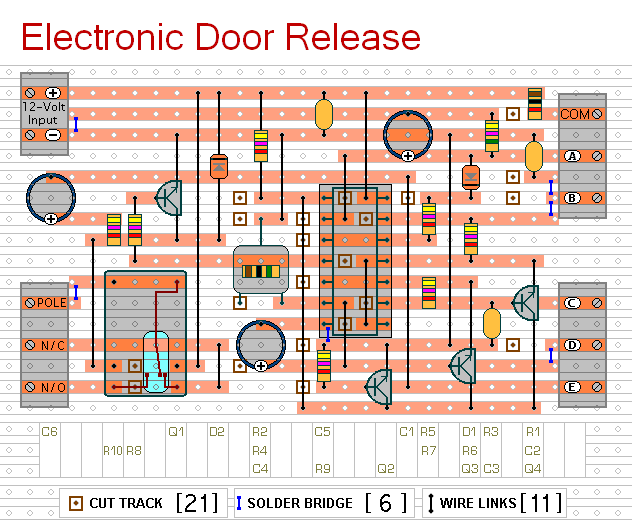
This circuit is designed to operate an electrical door-release mechanism, but it can be adapted for other applications. Upon entering a four-digit code of the user's choice, the relay will energize for a preset duration. The relay contacts can...