
Bootstrap Circuit
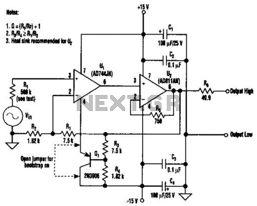
The bootstrapping technique in JFET amplifiers is a valuable method for enhancing linearity and reducing distortion. By employing a feedback divider that connects to the substrate of the JFET, the effective input capacitance can be stabilized, leading to improved performance. The resistor R1, valued at 500 kΩ, serves as a source impedance that plays a crucial role in this feedback loop.
In a typical JFET amplifier circuit, the input stage experiences variations in capacitance due to the non-linear characteristics of the JFET. These variations can introduce significant distortion, particularly at higher frequencies. By applying bootstrapping, the feedback divider adjusts the voltage at the substrate, effectively reducing the fluctuations in capacitance. This results in a more stable input impedance and a corresponding decrease in total harmonic distortion (THD).
The observed reduction in THD by an order of magnitude at 10 kHz indicates a marked improvement in audio fidelity and signal integrity. This enhancement is particularly beneficial in high-fidelity audio applications where clarity and accuracy are paramount. The implementation of this technique can lead to more reliable and consistent performance in JFET amplifiers, making it a preferred choice in precision electronic designs.
Overall, the integration of bootstrapping in JFET amplifier circuits exemplifies an effective strategy for mitigating distortion, thereby enhancing the overall quality of the output signal. Bootstrapping the substrate of a JFET amplifier reduces the distortion caused by the non-linlearity of the JFET input capacitance. In the figure, a second feedback divider bootstraps the substrate of Ul. With R{ = 500 kQ (source impedance), THD at 10 kHz was reduced an order of magnitude. 🔗 External reference
Related Circuits
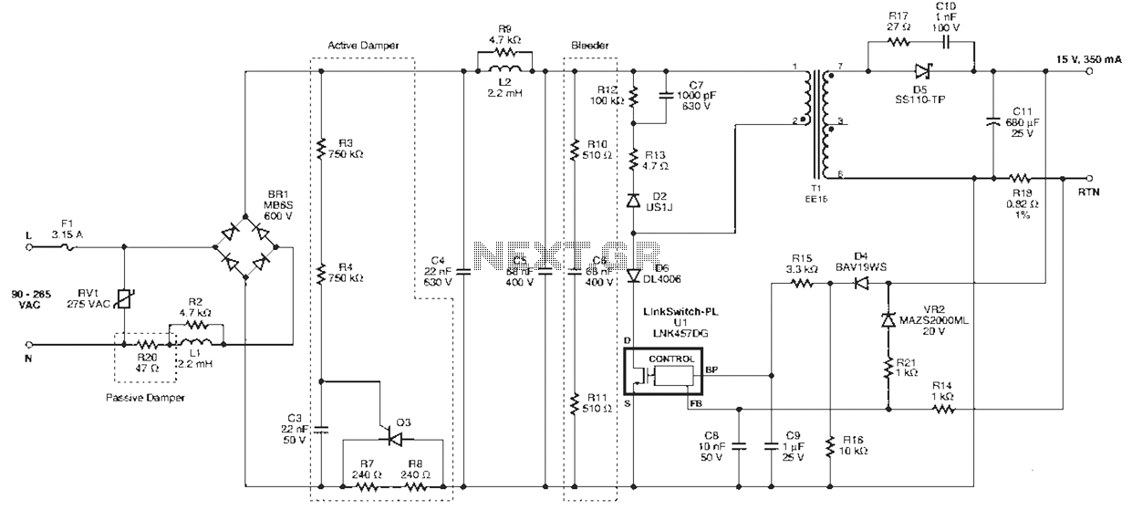
Power Integrations' DER322 reference design employs the LinkSwitch-PL family of LNK460VG devices. This design represents the industry's first alternative 100W A19 incandescent LED driver utilizing a single-layer PCB. It is characterized by low cost, minimal component count, and compact...
This document presents a collection of engaging and challenging electronic circuits that can be built for enjoyment. The author has a long-standing passion for electronics, having studied the subject since middle school and developed numerous circuits over the years....
An AC-DC power supply without a power switching circuit is typically utilized for lighting load circuits. Once the power grid is restored, the standby power supply automatically switches on. An automatic switching circuit using a transistor is implemented, with...

It was observed that balls were becoming lodged in the ball trough, failing to load into an upkicker or not resting correctly on the trough ball microswitches or optos, which caused the machine to register a missing ball. Initially,...
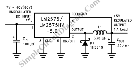
Switching Regulator for High Power Efficiency. When it is necessary to convert a high voltage to a significantly lower voltage, a switching regulator is the optimal choice. A switching regulator is an essential component in modern power management systems, particularly...
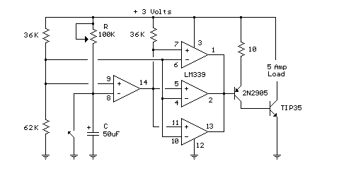
In this circuit, an LM339 quad voltage comparator is used to generate a time delay and control a high current output at low voltage. Approximately 5 amps of current can be obtained using a couple of fresh alkaline D...