
Buffer Circuit Schematic Diagram
The circuit utilizes a Darlington pair configuration for its buffer stage, which consists of two bipolar junction transistors (BJTs) connected in such a way that the current amplified by the first transistor is fed into the second transistor. This arrangement allows for a high current gain, making it suitable for applications requiring significant output current while maintaining low output impedance. The circuit's design ensures that the input signal is effectively buffered, preventing loading effects that could degrade signal integrity.
The resistor connected to the base of the first transistor plays a crucial role in setting the bias point of the Darlington pair, ensuring that it operates within its optimal range. This biasing resistor, denoted as R_base, helps stabilize the operation of the transistors and provides necessary current limiting to protect the components from excessive current draw.
The input voltage, Vin, is derived from a multivibrator circuit, which generates a square wave signal that serves as the clock signal for various digital applications. The operational voltage level of ±6V signifies that the circuit is designed to operate in a dual supply configuration, allowing for both positive and negative voltage swings, which is essential for certain types of digital logic circuits.
This buffer circuit's ability to handle high-frequency signals makes it suitable for applications in communication systems where signal integrity over long distances is critical. The low output impedance ensures that the buffer can drive multiple loads without significant voltage drop, which is vital in maintaining the quality of the clock signal across the bus system. Overall, the design emphasizes reliability and performance, making it an integral part of digital signal processing applications.The series is a series of input buffer equal to the output. In this is such a common collector circuit of air-reinforcement = 1. R value attached to restrict the current use is issued. Great value depends on the indication of its components, is usually not installed or flow is maximized in accordance with the op-amp capability. Buffer circuit here serves to reinforce the clock signal and synchronization for robust enough to be transmitted through a cable with a considerable distance. buffer circuit should have a fairly low output impedance. because the synchronization clock line and this is the track "bus" that is connected to a series of client (branch) in parallel.
output current should also be quite large, so as to move a few branches. output buffer in addition to pulse and synchronization signals can also be used as a source of supply. Buffer circuit using Darlington pairs that have the advantage as expected above. strengthening the buffer is quite high. R base serves as aretaining basis. Vin flow is the input voltage that comes from a series of MMV ( multivibrator). Where active at the level of ± 6V Vin = VCC. You are reading the Circuits of Buffer Circuit And this circuit permalink url it is 🔗 External reference
Related Circuits
Currently, the use of cookers has become fashionable due to their speed, cleanliness, and low pollution levels, making them a favorite among consumers. Cookers circuit. The modern cooker circuit typically involves a combination of heating elements, control systems, and safety...
A negative output voltage DC to DC converter generates a -5V output at pin A. To achieve -5V at point A, the primary of the transformer must fly back to a diode drop more negative than -5V. If the...
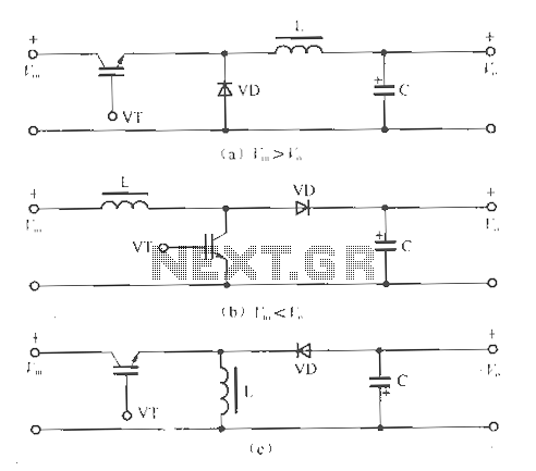
The circuit operates without isolation for both input and output voltage, utilizing a working switch along with an inductor (L), diode (D), and capacitor (C) to form a basic inverter circuit. There are three types of converters: the step-down...
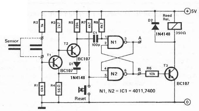
This humidity detector circuit diagram is straightforward and utilizes a limited number of components. It can be employed to activate electronic devices when the detector identifies a specific humidity level. The sensor is made from two copper pieces positioned...

This circuit generates sine and square wave signals with frequencies ranging from below 20 Hz to above 20 kHz. The advantage of this circuit diagram is that the output frequency can be adjusted by varying the variable resistor R6. The...
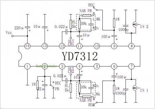
The YD9088 is a bipolar integrated circuit designed for use in mono portable and pocket radios. It is advantageous when minimizing peripheral components, which should be of small dimensions and low cost, is a priority. The circuit incorporates a...