
A non-isolated DC/DC converter circuit diagram

The circuit described encompasses three vital types of DC-DC converters: Buck, Boost, and Buck-Boost converters. Each type serves a specific purpose in voltage regulation and conversion, allowing for flexibility in various applications.
In the Buck Converter, the operation begins with the transistor VT switching on, allowing current to flow through the inductor L, which stores energy in the form of a magnetic field. During this phase, the output voltage Vo is lower than the input voltage Vin. The inductor current increases linearly until the transistor switches off, at which point the energy stored in the inductor is released through the freewheeling diode VD to the output load, maintaining a continuous current flow. This process results in a reduction of voltage while minimizing ripple by utilizing the filtering properties of the capacitor C, which smooths out variations in the output voltage.
The Boost Converter operates on a similar principle but aims to increase the voltage. When the transistor VT is turned on, the inductor L again stores energy. However, when VT is switched off, the energy stored in L is released, but this time it adds to the input voltage, resulting in a higher output voltage. The diode VD plays a crucial role in directing the current to the load and charging the capacitor C, which helps to maintain a stable output voltage.
The Buck-Boost Converter combines the functionalities of both the Buck and Boost converters, allowing for output voltage that can be either higher or lower than the input voltage. This versatility is particularly useful in applications where the input voltage may fluctuate above or below the desired output level. The configuration of this circuit involves careful selection of the inductor and capacitor values, as well as the control of the switching frequency to ensure efficient operation and minimal losses.
Overall, these converters are essential in modern electronic systems for efficient power management, enabling devices to operate under varying load conditions and input voltages while maintaining the required performance levels.For the input and output voltage without isolation but only with a working switch and L, D, C composed of an inverter circuit, its most basic form, the following three kinds: step-down converter (Buck Converter), boost transformation device (BoostConverter) and lower / boost: converter (Buck-boost converter). The circuit shown in Fig. 1. Buck Converter As shown in (a), 9 to reduce output ripple at the output of the access inductance L and capacitance C.
The figure for the freewheeling diode VD. Buck converter output voltage Vo is always less than the average of the input voltage Vin. Whether continuous inductor current iL, depending on the parameter value the switching frequency filter inductor L and capacitor C. When the higher operating frequency of the circuit, if the inductance of inductor values and capacitor capacitance is large enough, and after an ideal element, the circuit 9 may be considered steady state output voltage constant.
When the transistor VT conduction, the inductor current rises linearly; when the transistor VT off, the inductor current can not mutation induced electromotive force on the diode conduction. At steady state, the storm maintained a filter inductor DC component, eliminating the harmonic components, so the average value of the output current Io = Vo / RL ;, where RL is the load resistor.
2. Boost Converter Figure (b) shows a boost converter which converts the power transistors VT, the energy storage inductance L, capacitance C and filter diode VD composition. When the transistor VT turned on, the power supply to the inductive energy storage, the inductor current increases, the electromotive force of the left positive and right negative polarity, the load capacitance C power song.
When VT ended, the inductor current decreases, the polarity of the induced electromotive force negative right to left, the inductor releases energy, together with the input voltage via a diode VD power to the load while charging the capacitor C. Thus the high voltage and low voltage direct current into direct current. 3. down / step-up converter Figure (c) shows the reduction / boost converter, the output voltage Vo is greater than or less than the average value of the input voltage Vin, which is of opposite polarity.
Related Circuits
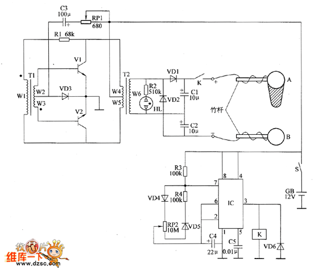
The electronic fishing shrimp machine circuit consists of an astable oscillator, an inverter circuit, and a high-voltage output circuit, as depicted in Figure 20. The astable oscillator circuit includes a time-base integrated circuit (IC), resistors R3 and R4, a...
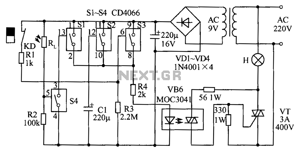
The circuit diagram illustrates a group of four analog electronic circuit switches (S1 to S4). Switches S1, S2, and S3 are utilized in a parallel delay circuit. When the power is activated, resistor R4 drives the triac VT, which...
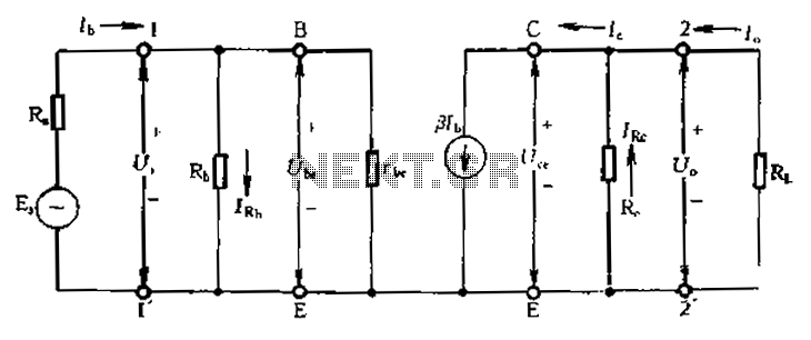
Calculate magnification, input resistance, and output resistance circuit. This circuit is designed to calculate the magnification, input resistance, and output resistance of a given electronic system. The magnification refers to the ratio of the output signal to the input signal,...
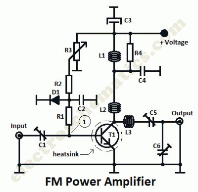
This is a 1 watt FM amplifier with a robust design that can be used to amplify an RF signal in the 88 to 108 MHz band. It is highly sensitive when utilizing quality RF power amplifier transistors, trimmers,...
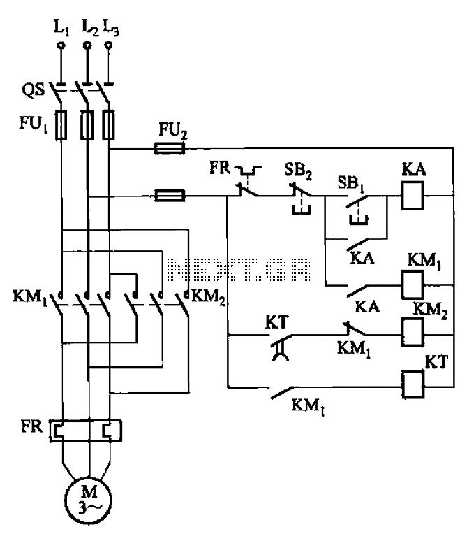
The circuit illustrated in Figure 3-127 utilizes a time relay (KT) in place of a speed relay. The timing duration is adjustable and typically set between 1 to 2 seconds. This circuit is designed to operate effectively in dusty...
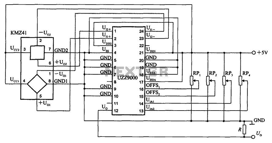
The UZZ9000 KMZ41 detection circuit is configured based on the voltage output type and angle. It operates with a +5V power supply. Potentiometers RP1 and RP2 are used for offset voltage adjustment, while potentiometers RP3 and RP4 are utilized...