
Car lights dimming circuit
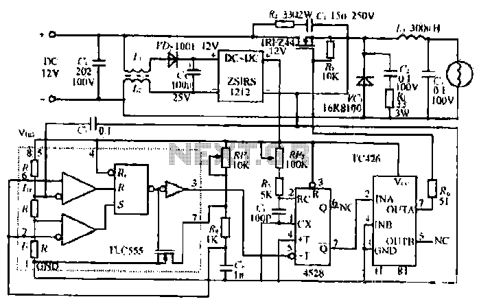
The schematic design features a Bute CD12V Lee output stage utilizing a high-performance MOSFET, specifically the BU1RF744, which is capable of handling significant current levels while maintaining low on-resistance (Rn(ON) = 0.028Ω). This MOSFET is configured to operate in a switching application, where it rapidly turns on and off to modulate the output voltage effectively. The circuit's operation is primarily controlled by a 555 timer configured in a monostable mode, which generates output pulses at a frequency of approximately 100 kHz, allowing for precise control of the MOSFET's switching behavior.
The timing circuit's output pulse width is adjustable, allowing for fine-tuning of the output voltage. The generated pulse is fed to the gate of the MOSFET, ensuring that it receives the necessary drive signal to switch states efficiently. The output voltage can be varied based on the resistance values in the circuit, achieving a maximum output voltage of approximately 12V.
To enhance the stability and performance of the power supply, the circuit includes a power supply filter capacitor, which helps to smooth out voltage fluctuations and reduce noise. Additionally, a common mode choke is integrated into the design to further suppress electromagnetic interference (EMI) and improve overall circuit reliability. The inclusion of a freewheeling diode provides a path for inductive kickback, protecting the MOSFET from voltage spikes during switching events.
Overall, this schematic provides a robust solution for applications requiring controlled power delivery with high efficiency and minimal noise, making it suitable for various electronic applications where reliable switching and voltage regulation are essential.1 Bute CD12V Lee output end of the eight-connected MOSFET power transistor BU * {1RF744) im JUV bone made this power MOSFET is turned on and should go off repeatedly called to ask L packet bundle coup output voltage, power on the pure silicon to cut lung width than the power MOSFET on the break, with house ... Orlando coefficient Cambodia large section of the output voltage is small, an analogue timing scarves 11.C555 foot waxy Jc, it is the gate to a frequency of about iOOkllz r hall is oscillation path.
Oh regulator R only "change vertical oscillation wave Hall {quite rate oscillator input side of the mountain crossing is intended to trigger the monostable multi-vibrator i travel all device 4528. rinse {il fog monostable multivibrator output pulse width on the world control J, [and raw coefficients, you can achieve the purpose of the coup when the output voltage Hl Rn resistance to deep house accounted for the largest d coefficient 100% power disobedient..
MOSFET all-i-turn, the output voltage is close J2V; ridicule .. m small m value decreases the space factor accounted Lan small pulse width to a few hundred microseconds turtle, the output voltage will be - left to play a single drop IV Liu Yan Zhi multivibrator. the end of the follow-up lotus then l rC426 to pay - booths built driver IC 'Gan I "W, j driving power MOSFET, etc.
- spin . explanatory power of the load circuit causes Cheng Chuan power transistor MOSFET (LRF244) drawer - species IrJ- . 50A, Rn (ON) = 0,028n high performance Jf Gou Fu pipe, the input capacitance of 19ffl) pF, Iti has been impossible to pass MOS lC-speed driving such roundworm cylinders are capacitive load - 0 compartment for the power supply filter capacitor zinc, DC - DC converter is a main power supply and the output terminal between Z f Gao holding isolation to reduce noise, then the common mode choke ,, r m L .; ridicule it .C, * and G scale is suppressed.
surge voltage buffer circuit access, I _ for the freewheeling diode.
Related Circuits
This circuit is designed for rapid battery charging. It is recommended for those who require a faster charger. The charger operates at a low temperature of 5 degrees Celsius. The input voltage is 15 volts DC, while the output...
This page is provided to the domain owner free of charge by Sedo's Domain Parking. The domain owner and Sedo do not have any relationship with third-party advertisers. References to any specific service or trademark are not controlled by...
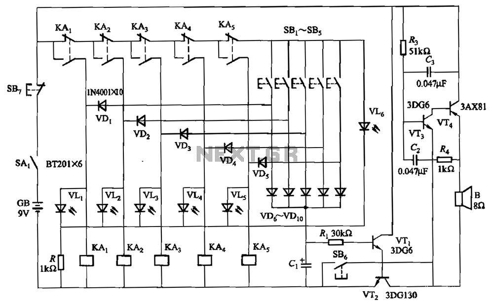
A relay-style circuit designed for a five electronic responder group. This circuit features self-locking capabilities, sound and light displays, time monitoring, and additional functions. The circuit includes a monitoring time button operated by the moderator. When this button is...

The SLB0586A integrated circuit from Siemens can be utilized to construct a straightforward touch light dimmer circuit, enabling the adjustment of lamp intensity. When paired with a TIC206D triac, this setup allows for smooth regulation of light intensity for...
This circuit design features a modular arrangement that enables users to select only the modules best suited to their needs, allowing for the construction of a chain ranging from one to five modules in length. For those seeking a...
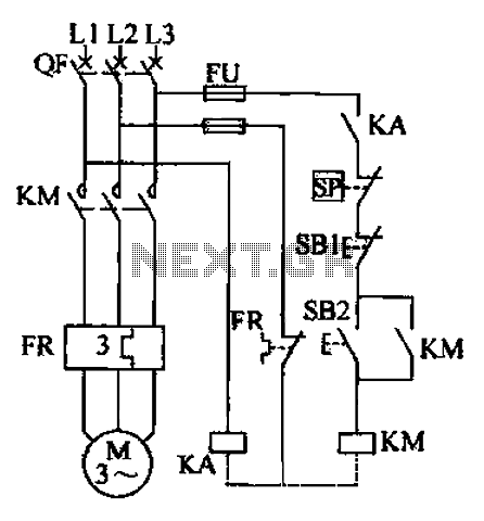
The air compressor control circuit operates based on several key principles. The first function is overload protection, which is facilitated by the thermal relay (FR). In instances of prolonged motor overload, the thermal relay activates to prevent overheating and...
Warning: include(partials/cookie-banner.php): Failed to open stream: Permission denied in /var/www/html/nextgr/view-circuit.php on line 713
Warning: include(): Failed opening 'partials/cookie-banner.php' for inclusion (include_path='.:/usr/share/php') in /var/www/html/nextgr/view-circuit.php on line 713