
Carrier Current Transmitter For Data Transmission

In this circuit design, the operational flow begins with the input signal at point C, which is processed by operational amplifier IC2. The purpose of IC2 is to amplify the input data to a sufficient level before it is sent to modulator IC1. The modulation process within IC1 is controlled by the logic level present at pin 9; a low signal generates frequency f1, while a high signal produces frequency f2. The specific frequencies generated are influenced by the passive components connected to IC1, including capacitors C5 and I10, and resistors R5, Rn, and R6.
The output from IC1 at pin 13 is a square wave signal, which serves as the input to the next stage, Q1. This transistor amplifier stage is crucial for driving the subsequent load. The output of Q1 is coupled to the AC line through a tuned transformer T, which ensures that the signal is properly matched and transferred to the line without distortion.
Additionally, capacitors C1 and C2 play a vital role in this circuit. They function as coupling capacitors that isolate the AC line from the rest of the circuit, preventing any DC offset from affecting the operation of the components. It is essential that these capacitors are rated appropriately for the AC line voltage to ensure safety and reliability in operation. Failure to use correctly rated components could lead to circuit failure or hazardous conditions.
Overall, this circuit exemplifies a typical application of modulation techniques in electronic design, where frequency generation and amplification are key to achieving the desired output signal characteristics. In this circuit, data at input C is amplified by IC2 and then fed to modulator IC1. IC1 g enerates two frequencies, depending on the values of C5, ii0, R$, Rn, and R6. The frequency/, is generated if pin 9IC1 is low and fa if pin 9IC1 is high. A square wave appears at pin 13 of IC1 and is fed to Ql, an amplifier stage, that is coupled via tuned transformer T, to the ac line via CI and C2. Notice that, for safety reasons, CI and C2 must be specifically rated for the ac line voltage.
Related Circuits
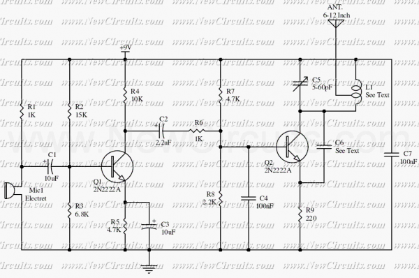
This circuit is a simple two transistor (2N2222) FM transmitter. No license is required for this transmitter according to FCC regulations regarding wireless microphones. If powered by a 9-volt battery and used with an antenna no longer than 12...
A resistance temperature sensor (RTD, resistive temperature device) is available in two types: NTC (negative temperature coefficient) and PTC (positive temperature coefficient). Resistance Temperature Detectors (RTDs) are essential components in temperature measurement systems. They operate on the principle that the...
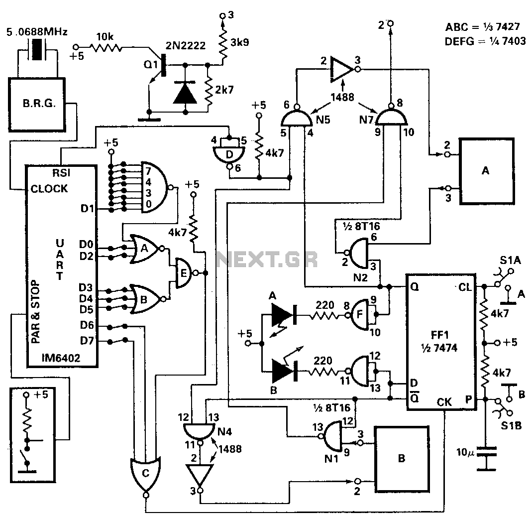
This data selector utilizes a single RS-232 port to connect two RS-232 devices (such as printers or plotters) to a mini or microcomputer. The operation is straightforward. When powered on, it resets FFI (QFFT ~ Low), which activates gates...
The LV2282VA is an FM Transmitter integrated circuit (IC). The multiplex (MPX) block generates a stereo modulated composite signal from left (L) and right (R) audio inputs. The radio frequency voltage-controlled oscillator (RF VCO) incorporates an FM modulation function....
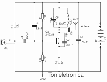
This small transmitter can reach distances of more than 1 km under favorable transmission conditions. Modulation can be achieved using a microphone, such as an electret microphone, or another audio source. The transmitter includes a coil made of 5...
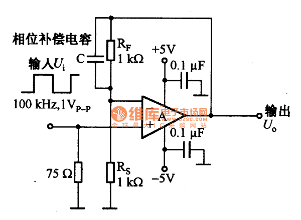
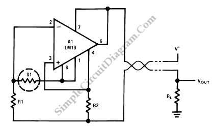
The current feedback operational amplifier maintains a consistent bandwidth even when the open-loop gain is altered. This characteristic makes it particularly suitable for applications in video signal amplification and the driving circuits of video cables. The accompanying diagram illustrates...