
Circuit diagram for generating time delay with 555 IC

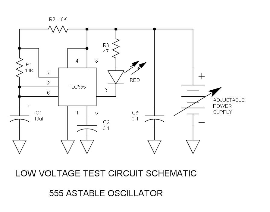
The NE555 timer is a versatile integrated circuit widely used in various timing applications. In astable mode, it operates as an oscillator, generating a continuous square wave output. The frequency of this output is determined by the resistors R1 and R2, as well as the capacitor C1. The relationship between these components and the output frequency allows for a wide range of adjustable timing intervals, making the NE555 suitable for applications such as LED flashing, tone generation, and pulse width modulation.
In practical applications, the selection of R1, R2, and C1 should consider the desired frequency and duty cycle of the output signal. The duty cycle, defined as the ratio of the high time to the total time period, can be adjusted by varying the resistor values. A higher resistance value for R1 will increase the high time, whereas increasing R2 will affect both the high and low times, allowing for fine-tuning of the output waveform.
For optimal performance, it is essential to ensure that the capacitor C1 is of suitable type and value, as this will influence the stability and reliability of the output signal. Additionally, bypass capacitors may be added to the power supply lines to filter out noise, ensuring that the 555 timer operates reliably in various environments.
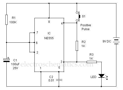
In summary, the 555 timer in astable mode is a powerful tool for generating precise timing signals, with applications ranging from simple LED blinking circuits to more complex timing and control systems. The flexibility in component selection allows for customization of the output characteristics to meet specific project requirements.This circuit based project demonstrates the working of 555 timer in astable mode to generate pulses of time period 0. 5 second. This pulse can be further used for anything where we need a pulse such as to blink a LED or to create fashionable blinking lights.
Image below shows internal circuitry of NE 555 timer which can be used in astable and monos table mode: This circuit of this project makes the use of timer IC NE555 which produces a constant square pulse of a desired frequency. This pulse could be either triggered or could be produced continuously depending upon the mode of 555 we are using.
The two mostly used modes of 555 are Monostable and Astable. Here it is used in the astable mode with time period of half second, with high time period of 0. 333 seconds and low time period of 0. 166 seconds. For astable mode total time period is [ln2C*(R1+2*R2)] with high time period as [ln2(R1+R2)*C]and low time period as [ln2(R2*C)]. Here R1 is the resistor connected between VCC and pin7 (discharge pin), R2 is between pin7 and pin2 (trigger pin) and C1 is the capacitor connected from pin2 to ground.
For 555 to function in astable mode pin2 and pin6 (threshold) pin must be shorted. Reset pin is connected to VCC. The output of 555 is taken at pin3 which is in the form of square wave and is then fed to lighting circuit which glows when output is high and stops when it becomes low; there by producing pattern of blinking lights. By varying the value of R1, R2 and C1 square waves of different time periods can be obtained. 🔗 External reference
Related Circuits
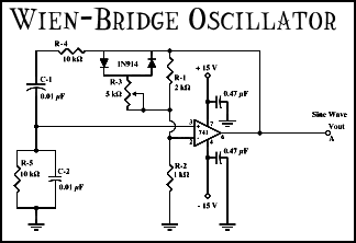
The Wien-Bridge oscillator meets specific requirements due to the presence of a low-pass filter, a high-pass filter, and a 180-degree phase shift from the feedback networks connecting the input to the output. This configuration results in a total phase...
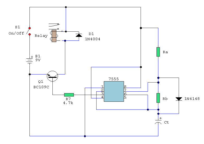
A simple astable timer made with the 555 timer IC allows independent adjustment of the mark (on) and space (off) values. The timing circuit comprises resistors Ra, Rb, and capacitor Ct. The capacitor Ct charges through resistor Ra, which...
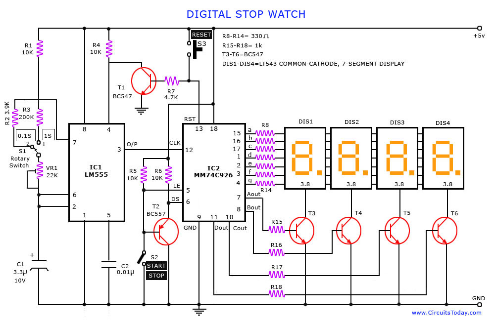
A digital stopwatch or digital timer circuit schematic is constructed using the timer IC LM555 and the 4-digit counter IC MM74C926, which is paired with a multiplexed 7-segment LED display. The digital stopwatch circuit utilizes the LM555 timer IC configured...
How many individuals have experienced legitimate issues with the 555 timer? It can be inferred that these problems often involve the reset line, specifically pin 4, which must be set high before operation. The 555 timer IC is a versatile...
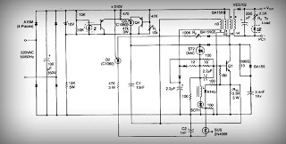
This is a low voltage, high-current output switching DC power supply with an input of 220 volts AC. In this circuit, an ST2 DIAC relaxation oscillator, Q3, C1, and the DIAC initiate conduction of the output switching transistor Q1....
This 555 timer is designed uniquely to provide a positive output through control over its reset pin. Typically, the 555 timer IC is triggered by applying a negative voltage. The 555 timer is a versatile integrated circuit widely used in...