2-to-1 Multiplexer
#multiplexer
#tristate buffers
#static inverter
#8-bit
#select bit
#logic design
#digital circuits
#data selection
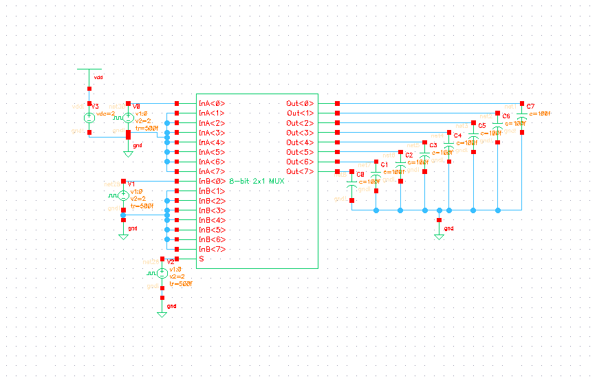
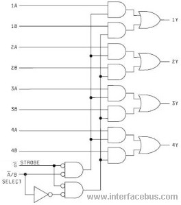
Description: The 8-bit 2x1 multiplexer comprises 16 tristate buffers and a static inverter. It is configured such that when the select bit is low, 8 of the input bits are transmitted through the tristate buffers to the 8 output bits. Conversely, when the select bit is high, the other 8 input bits are directed to the output. The static inverter is designed to be sufficiently robust to drive the 8 buffers it connects to. The worst-case conditions for this circuit indicate that the multiplexer achieved a rise time of approximately one nanosecond, with an additional nanosecond of delay observed between the input signal rising and the output signal beginning to rise. The falling output demonstrates a similar performance.
The 8-bit 2x1 multiplexer is a crucial component in digital electronics, allowing for the selection between two sets of input signals based on a single select line. This multiplexer utilizes 16 tristate buffers, which enable the control of the output state based on the select signal. When the select bit is low, the first set of 8 input signals is routed to the output, effectively enabling those signals while the other 8 inputs remain inactive. This is achieved through the use of tristate logic, which allows for the outputs to be in a high-impedance state when not selected, thus preventing signal contention.
The static inverter plays a critical role in ensuring that the tristate buffers receive adequate drive strength. Its design must accommodate the current requirements of the buffers to maintain signal integrity and minimize propagation delays. The inverter's performance is particularly important in high-speed applications where rapid switching is necessary.
In terms of performance metrics, the multiplexer demonstrates a rise time of approximately one nanosecond, indicating its capability to handle fast signal transitions effectively. Additionally, the observed delay of one nanosecond between the input and output transitions suggests that the design is optimized for minimal latency, which is crucial in high-frequency digital circuits. The symmetry in performance for both rising and falling edges indicates a well-balanced design, ensuring reliable operation in various signal conditions.
Overall, the 8-bit 2x1 multiplexer is an essential building block for digital systems, providing flexibility in signal routing while maintaining high-speed performance and low propagation delays.The 8-bit 2x1 multiplexer consists of 16 tristate buffers and a static inverter. It is designed so that when the select bit is low, 8 of the input bits are sent through tristate buffers to the 8 output bits, and when the select bit is high, the other 8 input bits are forwarded to the output. The static inverter was designed to be large enough to d rive the 8 buffers it is being sent to. * THE WORST CASE CONDITIONS FOR THIS ARE:. AS SHOWN IN OUR RESULTS BELOW, we got: The multiplexer acheived a rise time of roughly a nanosecond, with an additional nanosecond of delay between the time the input rises and the time the output starts to rise. The falling output achieves a similar result. 🔗 External reference
