
Combinational circuits Encoder Decoder

The encoder and decoder circuits play crucial roles in digital systems, particularly in data encoding and decoding processes. The decoder, operating on n-bit binary inputs, generates 2^n distinct outputs, which can be utilized in various applications such as memory address decoding, data multiplexing, and digital display systems. The enable signal is essential for controlling the circuit's operation, ensuring that the decoder only activates its outputs when required. This functionality is particularly useful in applications where multiple decoder circuits may be used in conjunction, allowing for selective activation based on system requirements.
The encoder, on the other hand, serves the purpose of compressing multiple input signals into a smaller number of output signals. In the case of an 8×3 encoder, it consolidates eight input lines into three output lines, effectively reducing the number of bits required to represent the input data. The outputs of the encoder represent the binary equivalent of the active input line, which is determined by the logic level of the inputs. This functionality is valuable in applications such as data transmission, where bandwidth conservation is essential.
Both circuits can be implemented using various logic gates, including AND, OR, and NOT gates, and can be designed to accommodate additional features such as priority encoding in encoders, where higher-priority inputs can override lower-priority ones. The design and implementation of these circuits require careful consideration of the desired functionality, input and output specifications, and the overall system architecture to ensure optimal performance in the intended application.The Encoder and Decoder are different kind ofcombinationalcircuits which are used to convert binary information to decimal, octal and hexa decimal andvice-versa. A decoder iscombinationalcircuitwhich is used for to convert n it binary information to 2n unique outputs.
so that a decoder circuit isused for to convert a binary information to de cimal, octal and hexa decimal. a decoder circuit is a variable circuit called as nxm decoder. The outputs are D0, D1, D2, D3, D4. The inputs are connected to 4 AND gates and derive Unique outputs. If we have Enable it will come along with input line. This is used to start the process of decoder circuit. Weather is Zero the inputs representing with xx called don`t care conditions. An encoder is a combinational circuit which is used to convert 2n inputs to n outputs. so that it is reverse operation of a decoder. it converts the decimal information to binary. In 8x3 encoder circuit consists 8 inputs called D0 to D7 and the outputs A0, A1, A2 the all the inputs connected to a specified OR gate to representing the binary equavalent of a specifed decimal. The outputs are as follows. 🔗 External reference
Related Circuits
Connect the serial cable to the serial port. If using a USB to TTL, RS232, or serial converter, plug it into the USB port. Next, short the Tx pin to the Rx pin or the TxD pin to the...
It is essential to consider migrating to PIC microcontrollers and exploring compilers such as those offered by Proton Smart, which include Sony IR and Philips RC5 codecs. This approach is particularly advisable for security-sensitive applications. Additionally, Bluetooth and Wi-Fi...
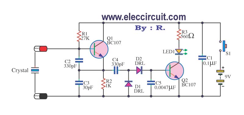
A multimeter cannot be used to test a crystal oscillator. Instead, a dedicated circuit is required, capable of checking crystals within the frequency range of 100 kHz to 900 MHz. This circuit is easy to construct and cost-effective. To construct...
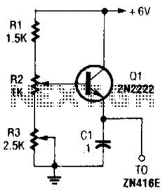
This regulator can be used with a +6-V source to supply the ZN416E low-voltage TRF radio receiver IC with the necessary +1.5 V. R3 sets the output voltage. The circuit utilizes a voltage regulator designed to convert a +6 V...

Several schematic drawings of battery charger circuits are provided. These circuits cover 5W to 200W for NiCd, NiMH, Lead-Acid, Li-Ion/Polymer, and LiFePO4 battery packs. The charger circuit files aim to assist users in selecting the appropriate chargers and to...
The phase shift oscillator produces a sine wave output in the audio frequency range. Resistive feedback from the collector results in negative feedback due to a 180-degree phase inversion from the base to the collector. The three 60-degree RC...