
IC Shift Register Chip
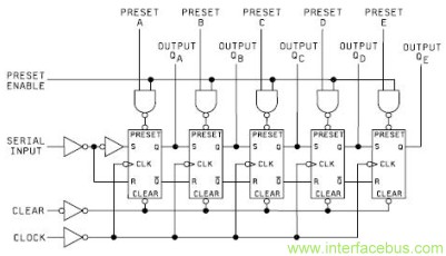
A shift register is a fundamental digital memory circuit used in various applications, including data storage, data transfer, and signal processing. The operation of a shift register is based on flip-flops, which are bistable devices capable of storing a single bit of data. In a typical configuration, a shift register comprises multiple flip-flops connected in series, with each flip-flop representing one bit of the data word.
The clock pulse serves as the synchronization signal that dictates when the data is shifted. When a clock pulse is applied, the data present in the flip-flops is shifted to the right, with the least significant bit moving into the first flip-flop and the contents of each subsequent flip-flop shifting to the next one. This shifting process can occur in two primary modes: serial and parallel. In serial mode, data is input one bit at a time, while in parallel mode, an entire data word can be loaded simultaneously.
The 74HC595, a popular shift register IC, is known for its high-speed operation and is part of the 74xx series of integrated circuits. This device features eight flip-flops and can be configured for both serial input and parallel output. The 74HC595 is particularly advantageous for applications requiring the expansion of output pins, such as driving LEDs or other devices. The device's architecture allows for cascading multiple shift registers, enabling the creation of larger data storage systems.
The pin configuration of the 74HC595 includes inputs for data, clock, and latch signals, as well as outputs for each of the eight bits. The latch function allows the stored data to be held stable while new data is being shifted in. The operational characteristics of the shift register, such as propagation delay and maximum clock frequency, are critical parameters that determine the performance of the circuit in real-world applications.
In summary, the shift register is a versatile component in digital electronics, enabling efficient data manipulation and storage. Its ability to operate in both serial and parallel modes, along with its compatibility with various IC families, makes it a fundamental building block in modern electronic systems.A shift register works by shifting data to the right with each clock pulse. Regardless of if the data is loaded in all at once via parallel load or one bit at a time via serial input. Each clock pulse shifts data into the first flip flop, the data that was in the 1st flip flop shifts to the 2nd flip flop and so on.
In a serial load shift register each flip flop begins with a 0 loaded. A parallel load shift register may contain what ever is loaded into the register when the load pin is activated. Regardless of what is pre-loaded, the data is shifted to the right with each clock pulse. IC 4-bit Shift Register Chip. A 4-bit serial in serial out shift register circuit is shown in the graphic above. Note that the shift register my be preloaded [preset] with data [parallel shift register]. However as shown below the 8-bit version is a bit more common. The 54xx military versions are shown above, but the components are available in the 74xx commercial version.
IC Commercial temperature ranges Industrial temperature ranges; by IC Family Prefix. A 74HC595 shift register is shown to the right, mounted on a printed circuit board. In other words a High Speed CMOS [HC] 595 shift register that operates within the commercial temperature range of 0 to 70 degree centigrade. The shift register circuit schematic above shows an 8-bit shift register having a serial input and a parallel output [parallel shift register].
The circuit represents a single 74164 Shift Register IC. The device is produced in a standard 14-pin Dual In-Line Package [DIP] or Leadless Chip Carrier [LCCC]. Refer to the IC pin out, lower right. The shift register circuit schematic above shows an 8-bit shift register having either a serial input or parallel input and a parallel output.
Similar to a 74165, or 74LS165. 🔗 External reference
Related Circuits
The prototype was successfully assembled on a breadboard and subsequently built on a piece of Radio Shack protoboard for field use. The assembly process took only a couple of hours, and it functioned correctly on the first attempt. This...
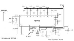
The following circuit illustrates a Single Chip FM Radio Circuit. This circuit is based on the IC TDA 7000 or TDA 7400. Features include a low-cost FM radio circuit. The Single Chip FM Radio Circuit utilizing the TDA 7000 or...
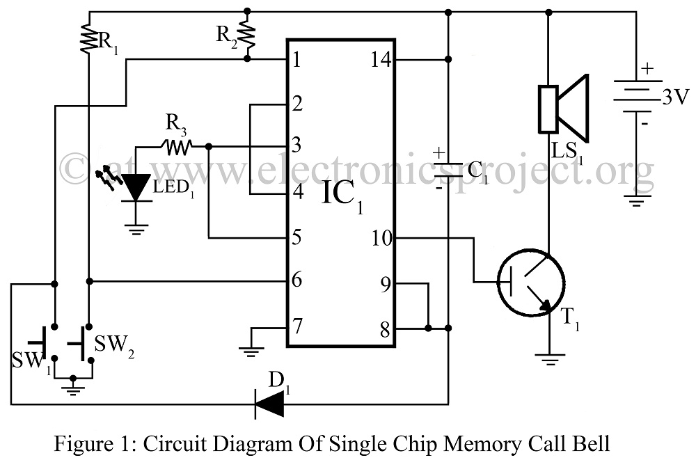
A single-chip memory call bell circuit utilizing a quad 2-input NAND gate (CD4011) that activates when a guest arrives in the absence of the homeowner. This circuit diagram includes various doorbell project configurations. The single-chip memory call bell circuit is...
This document illustrates the application of the MP3 player memory chip ACU7505 within a clamor circuit, designed to support the overall machine CPU and MP3 decoder core. The chip is utilized to address high data storage capacity requirements, implemented...
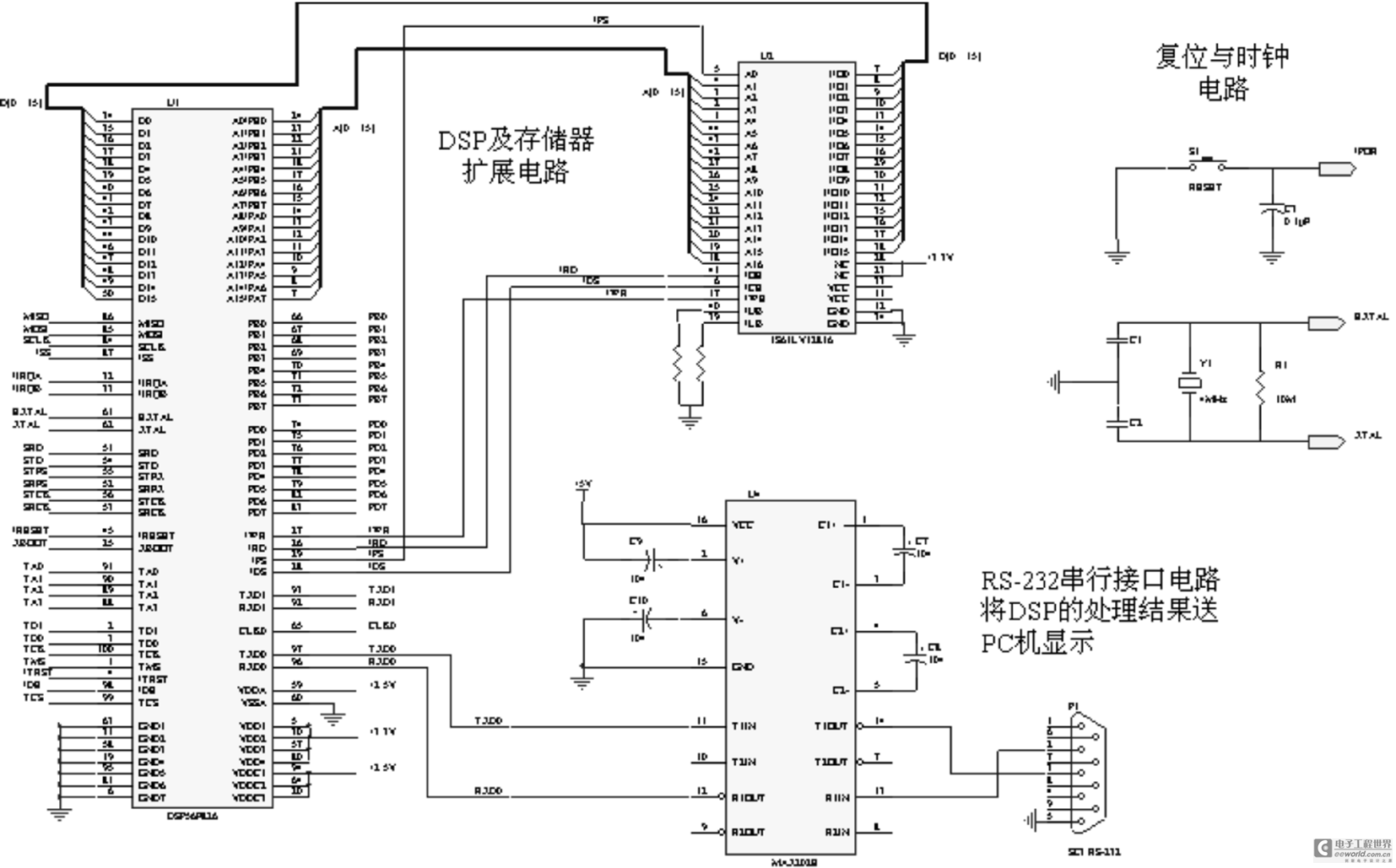
The system utilizes the DSP56F826 chip as the primary control module and incorporates a CMOS digital image sensor capable of capturing images with a resolution of 640 x 480 pixels. For applications requiring higher resolution, a chip supporting 1024...
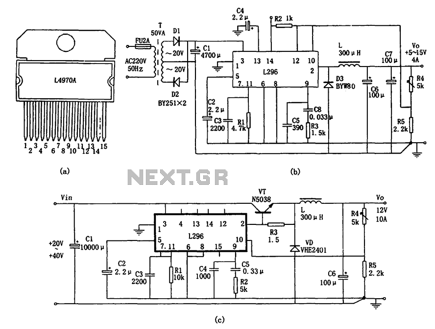
The L296 chip is a high-current switching power supply component designed to operate within a voltage range of 5 to 15V and provide an output current of up to 4A. This monolithic chip incorporates several features including enhanced protection...