
Clamp-on-current probe compensator

The clamp-on current probe configuration incorporates several key components designed to optimize performance across a range of frequencies. The operational amplifier N1 serves as the core of the signal processing unit, where its low-noise characteristics are critical for maintaining signal integrity. The feedback network, including C3 and R4, is strategically designed to enhance low-frequency response, effectively compensating for the inherent roll-off of the probe.
The choice of a low-noise operational amplifier like the LM725 is essential in applications where signal fidelity is paramount. To manage gain effectively, the circuit employs a feedback mechanism that adjusts the gain dynamically based on frequency. The values of C3 and R3 are crucial in defining the cutoff frequency, ensuring that the system remains responsive even at low frequencies while minimizing noise contributions.
The test square wave input of ±10 mA is a practical method for calibrating the probe's response. By observing the output waveform, adjustments can be made to the compensator PI to optimize the phase and amplitude characteristics, ensuring that the output remains stable without excessive droop or overshoot. This adjustment process is vital for achieving accurate readings when monitoring current waveforms.
At higher frequencies, the design anticipates a natural decline in response, commencing at 100 kHz. This characteristic is typical in many analog circuits and must be considered when selecting the probe for high-frequency applications. Overall, the integration of these components and their careful selection allows the Tektronix P6021 clamp-on current probe to function effectively across a wide frequency range, making it a valuable tool for electronic measurements.A clamp-on "current probe" such as the Tektronix P6021 is a useful means of displaying current waveforms on an oscilloscope. Unfortunately, the low-frequency response is somewhat limited, as shown in the Table. The more sensitive range on the P6021 is 2 mA/mV, but it has a roll-off of 6 dB per octave below 450 Hz.
The compensator counteracts the low-frequency attenuation, and this is achieved by means of C3 and R4 + PI in the feedback around op amp Nl. The latter is a low-noise type, such as the LM725 shown, and even so it is necessary at some point to limit the increasing gain with decreasing frequency; otherwise amplifier noise and drift will overcome the signal. The values shown for C3R3 give a lower limit below 1 Hz. A test square wave of ± 10 mA is fed to the current probe so that PI can be adjusted for minimum droop or overshoot in the output waveform.
At high frequencies, the response begins to fall off at 100 kHz. 🔗 External reference
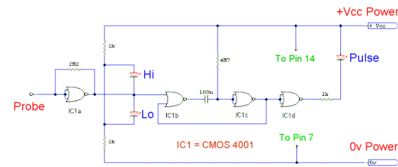
Related Circuits
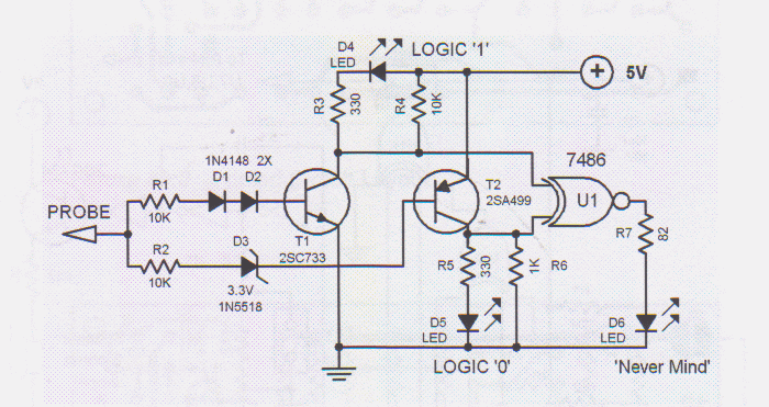
Logic testers are simple yet very useful devices for testing digital circuits. A logic probe can be designed in various ways. Logic testers, commonly referred to as logic probes, are essential tools in the field of digital electronics. These...
This logic probe utilizes a single CMOS integrated circuit (IC) to indicate three logic states: High, Low, and Pulsing. If the probe input is in a high impedance state, which occurs when it is not connected to a circuit,...
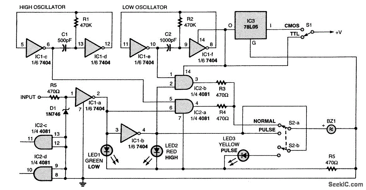
The figure illustrates the schematic for a versatile logic probe. The zener diode clamps the input signal slightly above the TTL inverter's 2.2-V trigger voltage. Zener diode D1 can be omitted if the probe is intended solely for use...
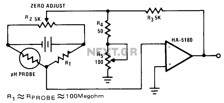
The highest sensitivity is attained when R1 is roughly equal to the probe resistance. The circuit can be calibrated to zero using R2, while R5 regulates the full-scale voltage. The relationship between pH and output voltage may not be...
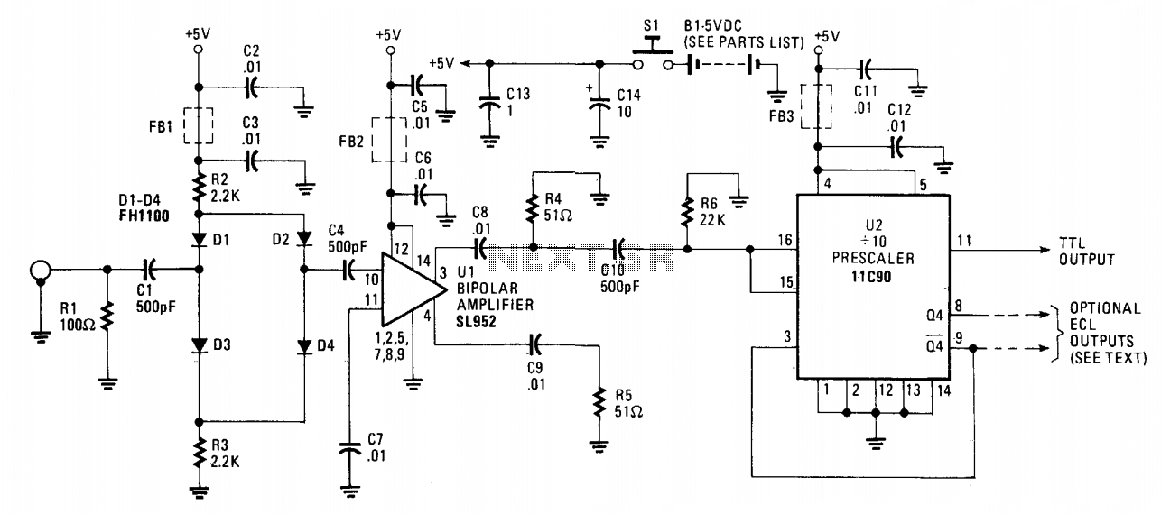
The 650 MHz prescaler probe's input is terminated by resistor R1 and is fed through C1 to the diode limiter composed of diodes D1 through D4. These diodes are forward-biased by the +5 volt supply for small input signals...
This circuit is so sensitive it will detect mains hum. Simply move it across any wall and it will detect where the mains cable is located. It has a gain of about 200 x 200 x 200 = 6,000,000...