
Pulse Reading Logic Probe
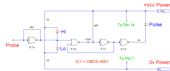
The logic probe circuit is designed for versatility and efficiency in testing digital logic levels. The CMOS technology allows for a wide operational voltage range, making it suitable for various logic families. The buffer configuration of IC1a is crucial for isolating the probe from the circuit under test, ensuring that the probe does not affect the logic levels being measured. The oscillation in the absence of an input serves as a useful diagnostic feature, indicating that the probe is operational and ready for use.
The integration of the monostable oscillator (formed by IC1b and IC1c) is a key enhancement, allowing the probe to handle rapid signal changes effectively. The time constant, determined by the selected capacitor and resistor, can be adjusted to cater to different signal frequencies, thus providing flexibility for the user. The output from the monostable oscillator ensures that even fast pulse signals can be visually represented by the LEDs, allowing for quick identification of signal conditions.
Overall, this logic probe design is a robust and efficient tool for electronics engineers and technicians, providing clear visual indicators for logic states and facilitating the testing of digital circuits across a range of supply voltages.This logic probe uses a single CMOS IC and shows three logic conditions, High, Low and Pulsing. In addition if the probe input is neither hi or low (the high impedance state of tri-output logic ic`s) then no LED`s will light. Power from the logic probe is taken from the logic circuit under test; using a CMOS IC enables logic circuits to be tested
using voltages from 3 to 15 volts. IC1a is arranged as a buffer with a difference. Under no input, i. e. probe not connected to circuit the gate will oscillate due to feedback from the 2M2 resistor. Output voltage at IC1a is approximately half supply voltage. The Hi and Lo logic indicator LED`s are also connected to a potential divider consisting of the two 1k resistors. Voltage at the junction is half supply voltage hence with no input, or high impedance no LED`s will light.
A Hi or Lo logic condition will cause IC1a to rest in a permanent state indicated by either the Hi or Lo LED illuminating. With a fast oscillator or clock signal both Hi and Lo LED`s will light but will be quite dim. This is the reason for IC1b and IC1c. These two gates form a monostable oscillator, time constant determined by the 100n capacitor and 4M7 resistor.
With a clock signal this is effectively slowed as the monostable is continually triggered and retriggered. IC1d acts as a buffer to drive the pulsing LED. 🔗 External reference
Related Circuits
One of the primary objectives was to convert a generator into a motor using an Arduino. The process of transforming a simple generator into a motor proved to be particularly challenging with a three-phase generator, necessitating the creation of...
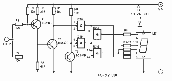
This tester, the logic level digital signals indicate on a 7-segment display. The display shows an H as the input signal is high. When the signal is low, the display shows an L on. If the input is open,...
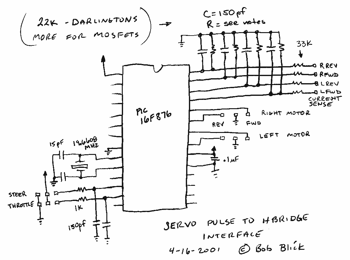
The interface uses a PIC16F876 microcontroller and not much else. It performs channel mixing, current limiting, and noise rejection. Push the stick forward, both motors move forward, move the stick to the left and the robot moves left. It...
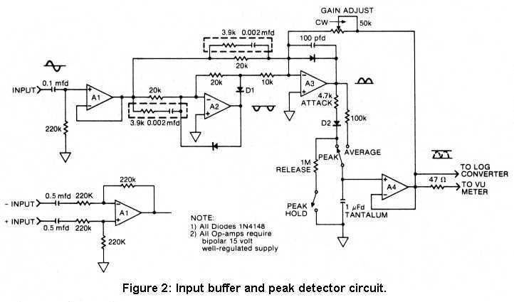
Peak reading meters, popular in Europe for years, are just now coming into greater favor in America, and for good reason. The main purpose for having a VU meter is obviously to monitor signal levels going to a tape...
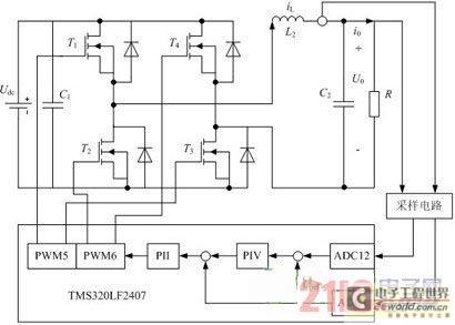
Traditional UPS systems use analog circuit control, which presents significant limitations for both manufacturers and users, regardless of whether they employ technology or SPWM technology. With advancements in information technology, the introduction of high-speed digital signal processing chips, known...
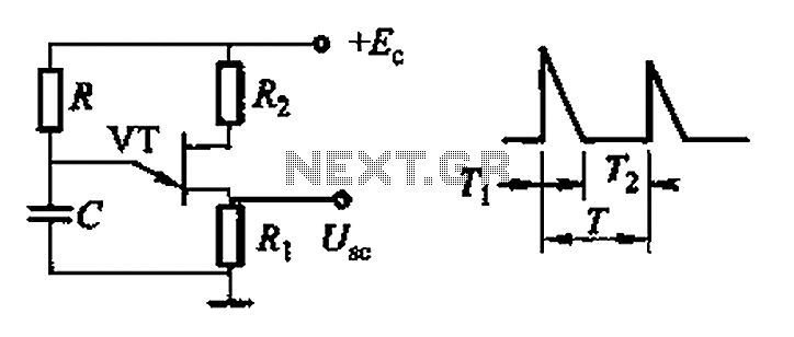
Common non-sinusoidal oscillator circuit, waveform and frequency formula - pulse wave oscillator - blocking oscillator transformer The common non-sinusoidal oscillator circuit is designed to generate pulse waveforms, which are characterized by their square or rectangular shape. These oscillators are...