
Class A 40W into 8 Ohms Amplifier
Parts List (each channel)
R1 2k2 , all resistors RN55D metal film 1% 1/4W
R2 10k
R3 330 ohms
R4 100 ohms
R5 10k
R6 680 ohms
R7 330 ohms
R8, 9 470 ohms
R10 100 ohms
R11 4k75
R12 750 ohms
R13 2k2
R14, 15 68 ohms
R16-19 0.68 ohms, 1W, 5% wirewound
R20 10 ohms, 1W, 5% Carbon comp.
R22 10 ohms
C1 300pF, 50V, 5% silver mica
C2,3 220uF, 10 V tantalum
C4 40pF, 5%, 500V silver mica
C5 0.1uF, 100V, mylar
Q1-4 MPSL 01 Motorola
Q5 MPSL 51 Motorola
Q6 MPSL 01 Motorola
Q7,8 PMD16K100 Lambda
Q9,10 PMD17K100 Lambda
D 1-3 1N4148 diode
Q11 2N5248 FET
Da,b 25A 100piv bridge
Ca-d Capacitors, 35V, Computer grade
Ce,f 0.01uF, 1500V
S1 SPST switch, 10A
F1 10A, fast-blo
F2-4 3A, fast-blo
T1 Signal 88-8, Pri: 118V, Sec: Two 44V, CT, 8A. Alternate: 2 Transformers with 44V, CT, 6A
Heat sinks (two per channel) Thermalloy #6560, 6590, 6660, 6690, or equiv. DAMPING, CURRENT, OUTPUT
Fig. 7 illustrates the output damping factor of the amplifier versus 8 Ohms (disregarding the impedance of the output fuse) and shows the effects of the open loop rolloff with lead compensation versus the same capacitor used to lag Q5. The high, wide-band damping factor serves particularly well into low impedance, especially reactive loads.
The two current sources formed by Q3 and R7, and Q4 and R10 are driven by the voltage source D1 and D2, which is a reference voltage diode pair producing 1.3V when forward biased by the current flowing through the current source FET Q11. This 1.3V at the base of Q3 results in a .6V drop across R7, yielding a current source value of 2mA. Q4 operates at 6mA (.6V)/(100 Ohm) with the addition of R8, which prevents the reference voltage from collapsing when Q4 saturates during a negative clip, thereby improving the recovery time.
Q11 and R8 also serve to feed current to diodes D1 and D2, providing the voltage reference for the current sources. Q11 and R8 form a current source themselves, and used instead of a resistor to bias the diodes, they provide higher power supply rejection for the negative half of the circuit, lowering ripple voltage noise and distortion by about 20dB.
The amplifier performs well under sinusoidal testing. The correlation of these results to transient conditions is significant. Traditional testing procedures may not fully capture the nuances of sonic performance, but the distortion waveform of an amplifier reveals much about transient performance.
Apart from slew rate, amplifiers often face challenges with reactive low impedance loads found in crossover networks or electrostatic speakers. For instance, the amplifier's capability into such loads is demonstrated in the response to a 10kHz plus and minus 10V square wave into a 2uF and 1uFBoth parts of the circuit are biased with the constant current sources as shown, and the signal from the collector of the PNP is followed by the Darlington class A output stage whose idle current is controlled by the bias circuit. The transistors Q1 and Q2 form the traditional differential pair but there are some twists added to the feedback and input networks.
The feedback circuit formed by R3 R4 R5 C2 C4 is used to bootstrap the input impedance to a nominal value of 40k Ohms while providing a low impedance path for the input bias currents. This results in a high input impedance with low offset voltage. The capacitor C4 creates a high frequency input to the negative feedback circuit which rolls off the high frequency gain of the amplifier.
C4 frequency compensates the amplifier by creating internal feedback which allows the front end of the amplifier to work at satisfying the high frequency loop requirements by itself, ignoring the phase effects of the output stage and providing a high degree of stability for the system. As a form of feedforward technique, it does not impair the slew capabilities as lag compensation would, and comes into play at around 200kHz.
The Pass A40 Power Amplifier The Audio Amateur 4/78 by NELSON PASS FLATTERED BY THE opportunity to publish a project circuit, the designer is often beset by seemingly contradictory considerations. On the one hand, it is tempting to design a complex circuit as a demonstration of technical prowess; an amplifier with large numbers of esoteric components performing obscure functions.
Such an amplifier might be a smorgasbord of electronic technique, featuring class A operation, cascoding, constant current sources, current mirrors, and extra-loop error correction. It would be fascinating to build and perhaps would also sound good. On the other hand, complexity is not a good end in itself and a much simpler circuit would suit the needs of the amateur more ideally for low cost, high reliability, and easy construction.
Simplicity can often yield sonic benefits, inasmuch as the fewer the number of components in a signal path, the simpler the open loop transfer curve of the amplifier. The importance of a simple transfer curve accounts partially for the high quality of sound in many tube type devices.
Their simple circuitry assures a higher concentration of low order distortions, 2nd and 3rd harmonics and 1st and 2nd order intermodulations, giving them a pleasant musical sound even at relatively high distortion levels. By contrast, the higher order distortions to be found in many poorly biased solid state amplifiers are less musical and thus more detectable.
This effect is similar to one's ability to detect a scraping voice coil on a woofer more easily than a much higher percentage of 2nd harmonic in the woofer. While this is partly due to the unmusical nature of these overtones, it is also due to a fault in the measurement technique which assumes that our ears are average responding, like the meter on the distortion analyzer.
A good example is crossover notch {the amplifier's equivalent of a scraping voice coil}, which is a spike of distortion occuring when the transistors are switching the signal from the positive set to the negative set and back again. Because it only occupies a brief percentage of the operating cycle, crossover notch distortion can occur in very high peaks which then are averaged down to a much lower figure, giving a misleading impression of the audibility.
Does the ear respond to such brief distortions? I don't know, but it is true that amplifiers with nearly identical "standard" specifications can sound different and it seems that low versus high order harmonics and intermodulation are one common key to the sonic disparity. Fewer elements in series with the signal path also result in wider bandwidth and greater stability, as there are fewer contributions to the high frequency rolloff of the circuit.
PERFORMANCE VS. PARTS Given then that the circuit should be simple, we must find a way to achieve the exceptional performance as advertised. While we want simple distortion types, we also want a lot less of them, which brings us to the question: what techniques will extract maximum performance from a few parts?
In this case I have chosen two very effective approaches: constant current sourcing and class A operation which are combined in a deceptively simple 40 Watt per channel amplifier. Constant current sourcing is a technique used to achieve high gain and linearity by biasing transistors heavily without loading down the gain as a resistor current source would.
A constant current source delivers a specified value of DC current regardless of the fluctuations of the power supply or the voltage swing of the amplifier, resulting in less distortion and noise. Constant current sources may be formed in a number of ways, one of the most popular being the circuit for Fig.1 where the forward voltage drops of the PN junctions is used as a reference to drive about .7 Volts across a resistor.
This voltage across the resistor causes a constant current to flow through the collector/emitter path of the transistor which is independent of the voltage at the collector between saturation and breakdown. Of particular value in linear circuits, constant current sourcing sets up conditions where the device's operation moves it about its operating point by only a small percentage of its capability.
WHY CLASS A? Class A operation is integral to the performance in this case, and it is worthwhile to explore why. The primary virtue of class A lies in the smooth characteristics of its operating parameters. The gain transistors are operated in their linear region only, where the distortions are limited to smooth, simple forms, unlike the abrupt distortions created when the transistors in class B output stages switch on and off. In class A, the transistors are always on, eliminating the turn-on/turn- off delays which characterize the crossover of class B and even AB amplifiers.
The distortion is inherently lower without the need for cleaning up via feedback, thus class A lends itself well to low distortion performance in a simple circuit with low open loop gain. Fig. 2 shows the transfer curves for a push-pull emitter follower output stage operated in class A, B. and AB modes where the crossover distortion is apparent in the discontinuity of the curve. In class AB, this effect is alleviated by a small bias current, and then is eliminated in class A where the bias current is high.
Fig. 3 shows the open loop output impedance of these stages where the class B amplifier is seen to rise abruptly at the discontinuity, whereas the class AB actually drops at the point where both halves conduct current. The class AB amplifier can be said to run in class A over this small region and will exhibit class A performance at small current levels.
The class A curve can be observed to be the smoothest of the three in an effect which can be looked upon as the damping factor of the amplifier multiplied by the amount of feedback employed. Naturally, this kind of performance has a price tag, and with class A operation, the low efficiency causes considerable energy loss.
Class A power amplifiers require large power supplies to handle this energy, but the task is not as enormous as might be imagined. BEATING THE HEAT Class A amplifiers have different efficiency factors depending upon the design. The least efficient is the circuit of Fig. 4a, where the transistor is biased by a resistor and whose AC output power to the load is less than 20 per cent of its idling dissipation.
Fig. 4b shows the same configuration where a constant current source replaces the resistor, improving the linearity and efficiency of the circuit. The value of the constant current source must be equal to or greater than the maximum output current.
For an 80W peak (40W, rms) into 8 Ohms, therefore, the current must be at least 3.2A, which practically speaking means a worst case dissipation of 200W per channel in the idling output stage. Push-pull circuitry more or less doubles the efficiency of a class A output stage (Fig. 4c) because unlike the constant current sourced design, its idle current need be only one half the peak output current, or 1.6A in the example, for an idling dissipation of about 100W for a 40W amplifier.
At these power levels, we will expect some degree of heat and will need to figure out the amount of cooling required. If we assume a 25° C. ambient temperature, for each channel we will require a heat sink with a .25° Celsius per Watt thermal characteristic.
This can easily be made from two .50° C./Watt sinks or four 1° C/W sinks, remembering that air should flow vertically along the fins on the sink and that some free space must be available on all sides of the heat sink, especially top and bottom. With this much sinking, the 100W idling dissipation will raise the sink temperature at 25°C above ambient for a temperature of 50°C.
This is easily handled by the four output transistors whose cumulative dissipating capabilities are 600 Watts at this temperature. The 6:1 safety margin here may cause some readers to wonder if I wear both a belt and suspenders, but in my experience, textbook safe operating areas are somewhat optimistic.
In real life circuits with a 2:1 safety margin generally blow up. HEAT AND ECOLOGY Contrary to popular belief, class A output stages are not necessarily subject to thermal runaway. Whereas class AB amplifier designers often invest in thermal compensation to correct the delicate bias voltage, class A output stages use a gross bias current without much need for small adjustment.
The high bias currents develop significant voltages across the transistors' emitter resistors, reducing the temperature dependence of the bias. In addition, this amplifier incorporates an interesting bias circuit which senses the idling current of a class A output stage while ignoring the AC signal and maintains a constant bias without need for adjustment.
One nice thing about hefty output stages as found in class A operation is that often no protection circuitry is required beyond a fuse because of the excellent thermal capability of the bank of transistors. This same capability yields better performance into demanding loads and holds the transistor chips at a more constant temperature than the flimsier output stages found in class AB amplifiers.
Nevertheless, I must admit that class A operation consumes energy which is converted to the heat emitted by the amplifier. While its consumption is about on a par with a large color television, the ecologically oriented audiophile may wish to operate his class A amplifier only during the winter, when he would otherwise be using his heater, and revert to a class AB design amplifier during the summer.
DESIGN ANALYSIS The conceptual schematic for the amplifier is given in fig. 5, where you can see the rather conventional NPN differential front end which drives a PNP voltage gain transistor. Both parts of the circuit are biased with the constant current sources as shown, and the signal from the collector of the PNP is followed by the Darlington class A output stage whose idle current is controlled by the bias circuit.
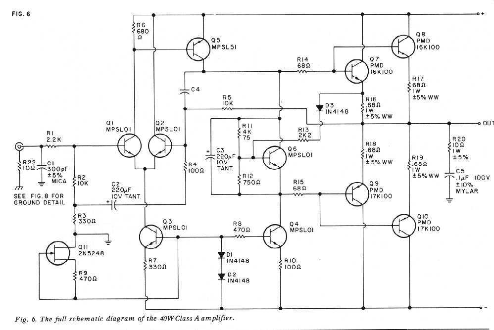
Breaking down the schematic of the actual unit of Fig. 6, we start with C1 forming an input rolloff filter in conjunction with the typical 600 Ohm to 1k Ohm source impedance. Lower frequency rolloffs can be achieved using higher capacitance values and higher source resistance values.
The transistors Q1 and Q2 form the traditional differential pair but there are some twists added to the feedback and input networks. The feedback circuit formed by R3 R4 R5 C2 C4 is used to bootstrap the input impedance to a nominal value of 40k Ohms while providing a low impedance path for the input bias currents.
This results in a high input impedance with low offset voltage. The capacitor C4 creates a high frequency input to the negative feedback circuit which rolls off the high frequency gain of the amplifier. C4 frequency compensates the amplifier by creating internal feedback which allows the front end of the amplifier to work at satisfying the high frequency loop requirements by itself, ignoring the phase effects of the output stage and providing a high degree of stability for the system.
As a form of feedforward technique, it does not impair the slew capabilities as lag compensation would, and comes into play at around 200kHz. Parts List (each channel) R1 2k2 , all resistors RN55D metal film 1% 1/4W R2 10k R3 330 ohms R4 100 ohms R5 10k R6 680 ohms R7 330 ohms R8, 9 470 ohms R10 100 ohms R11 4k75 R12 750 ohms R13 2k2 R14, 15 68 ohms R16-19 0.68 ohms, 1W, 5% wirewound R20 10 ohms, 1W, 5% Carbon comp.
R22 10 ohms C1 300pF, 50V, 5% silver mica C2,3 220uF, 10 V tantalum C4 40pF, 5%, 500V silver mica C5 0.1uF, 100V, mylar Q1-4 MPSL 01 Motorola Q5 MPSL 51 Motorola Q6 MPSL 01 Motorola Q7,8 PMD16K100 Lambda Q9,10 PMD17K100 Lambda D 1-3 1N4148 diode Q11 2N5248 FET Da,b 25A 100piv bridge Ca-d Capacitors, 35V, Computer grade Ce,f 0.01uF, 1500V S1 SPST switch, 10A F1 10A, fast-blo F2-4 3A, fast-blo T1 Signal 88-8, Pri: 118V, Sec: Two 44V, CT, 8A. Alternate: 2 Transformers with 44V, CT, 6A Heat sinks (two per channel) Thermalloy #6560, 6590, 6660, 6690, or equiv.
DAMPING, CURRENT, OUTPUT Fig. 7 plots the output damping factor of the amplifier vs. 8 Ohms {disregarding the impedance of the output fuse) and shows the effects of the open loop rolloff with the lead compensation versus the same capacitor used to lag Q5. Fig. 7 also shows the high, wide-band damping factor, which serves particularly well into low impedance, especially reactive loads.
We see also in Fig. 6 the two current sources formed by Q3 R7 and Q4 R10. They are driven by the voltage source D1 D2 which is a reference voltage diode pair which produces 1.3V when forward biased by the current following through the current source FET Q11. This 1.3V at the base of Q3 results in a .6V drop across R7, giving the current source a value of 2mA.
Q4 thus operates at 6mA (.6V)/(100 Ohm) and has the addition of R8, which prevents the reference voltage from collapsing when Q4 saturates during a negative clip, improving the recovery time. Q11 and R8 serve to feed current to the diodes D1 D2 which provide the voltage reference for the current sources.
Q11 and R8 form a current source themselves, and used instead of a resistor to bias the diodes, they provide a higher power supply rejection for the negative half of the circuit. This lowers ripple voltage noise and distortion by about 20dB. The amplifier performs well under sinusoidal testing, and the reader may well wonder how this correlates to testing under transient conditions.
While traditional testing procedures have not impressed most audiophiles for their exactness in a description of sonic performance, this is not the fault of the test procedure, but our interpretation of the data. The wealth of information received from the distortion waveform of an amplifier certainly should not be processed into a single number as it reveals much about "transient" performance.
Apart from slew rate, amplifiers often encounter problems associated with reactive low impedance loads found in crossover networks or electrostatic speakers. As an example of this amplifier's capability into such loads Fig. 21 shows a 10kHz plus and minus 10V square wave into a 2uF, 1uF capacitor, showing a small amount of well damped ringing generated by the wire's inductance.
To gain a greater appreciation of the demand this places on an amplifier, Figs. 22A and 22B show the response of the amplifier to step functions where an additional trace shows the amount of current output of the amplifier simultaneously with the voltage output. (Vertical: top: 10V/div; bottom: 10A/div; horizontal: 10us/div.) From them, we see that the amplifier is delivering nearly 15 Amperes under high slew conditions without waveform breakup.
The amplifier has been tested into the modified Dayton Wright XG8 MK IIIs whose impedance is .5 Ohms from 4kHz to 20kHz, without problems. It even sounds good. In summary, here is a simple but excellent amplifier which I hope some of you will build. While a few of the parts are exotic, Old Colony Sound will be offering them as a partial kit, which should take care of the problem.
Remember, an amplifier does not have any particular memory, and does not differentiate between a sinusoidal or a pulsed waveform - it is merely going where it is sent. "Steady state" distortion, or distortion at lower frequencies, reflects how accurately the voltage is placed, and transient distortion reflects how rapidly it can be placed.
Q7-10 are special complementary Darlington transistors, chosen especially for their rugged safe operating area and the 25 Ohm value of their internal driver's emitter resistor. These cannot be adjusted by the user and most manufacturers use about 100 Ohms in this spot, which results in far less bias on the driver transistor.
Q1-4 MPSL 01 Motorola Q5 MPSL 51 Motorola Q6 MPSL 01 Motorola Q7,8 PMD16K100 Lambda Q9,10 PMD17K100 Lambda D 1-3 1N4148 diode Q11 2N5248 FET 🔗 External reference
Related Circuits
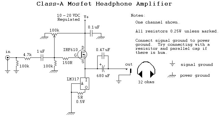
Dissatisfied with the performance of a computer soundcard when driving 32-ohm headphones, a decision was made to construct a Class-A MOSFET headphone amplifier. The objective was to maintain simplicity, minimize costs, and utilize salvaged components whenever possible. This project...
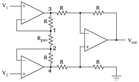
It is advantageous to adjust the gain of an amplifier circuit without modifying more than one resistor value, unlike the previous design of the differential amplifier. The instrumentation amplifier builds upon the last version of the differential amplifier to...
Modern sound systems often lack inputs for record players, leading to a rise in the popularity of separate MD preamplifiers. These devices are essential not only for vinyl enthusiasts but also for individuals looking to digitize their LP collections...

This is a stereo audio amplifier circuit that delivers 12W output power for each audio channel. The circuit is constructed using a single integrated circuit, the TDA1521 or TDA1521Q, and is supported by a minimal number of external components. The...
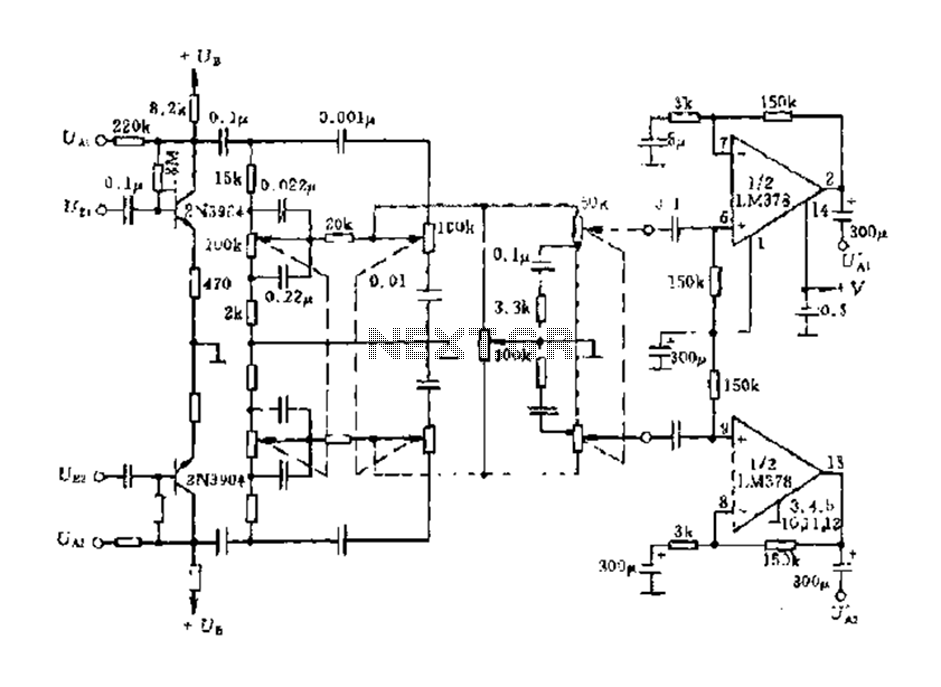
The dual-channel circuit features the LM378 dual operational amplifier and operates with a supply voltage of 24V, supporting an 8-ohm load (or 16 ohms). Each channel delivers an output power of 4W. The circuit includes internal current limiting and...
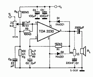
The TDA2030 is a monolithic integrated circuit in a Pentawat® package designed to function as a Class AB audio amplifier. It typically delivers up to 14 watts of output power (with a distortion rate of 0.5%) at 14V with...
Warning: include(partials/cookie-banner.php): Failed to open stream: Permission denied in /var/www/html/nextgr/view-circuit.php on line 713
Warning: include(): Failed opening 'partials/cookie-banner.php' for inclusion (include_path='.:/usr/share/php') in /var/www/html/nextgr/view-circuit.php on line 713