
CMOS interface circuit with the PMOS cross-c
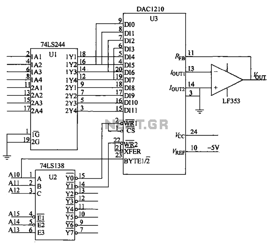
The CMOS interface circuit utilizing PMOS cross-coupled configurations is designed to achieve high input impedance, making it suitable for applications where minimal loading on the preceding stage is critical. The PMOS transistors in this configuration operate in a complementary manner, allowing for enhanced performance in terms of noise margins and power consumption.
In this circuit, the PMOS transistors are arranged in a cross-coupled manner, which provides improved stability and reduces the susceptibility to variations in temperature and supply voltage. The high input impedance characteristic of this configuration is primarily due to the inherent properties of PMOS transistors, which exhibit low gate leakage currents. Consequently, the input current can be considered negligible, allowing for accurate signal processing without significant distortion or attenuation.
The CMOS interface circuit can be employed in various applications, including analog signal processing, sensor interfacing, and as part of more complex digital systems. The circuit's design typically includes biasing networks to ensure optimal operating conditions for the PMOS devices, as well as decoupling capacitors to filter out noise from the power supply.
In summary, the described CMOS interface circuit with PMOS cross-coupled transistors provides a robust solution for interfacing high-impedance sources while maintaining low power consumption and high signal integrity, making it an essential component in modern electronic designs. CMOS interface circuit with the PMOS cross-c PMOS integrated circuit high input impedance, input current can be ignored. CMOS and PMOS interface circuit shown in Figure
Related Circuits
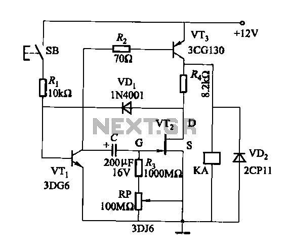
Discharge time relay circuit. The timer utilizes a field effect transistor, providing high timing accuracy and extended timing capabilities. With R3 set to 1,000,000 ohms and C at 200 microfarads, a delay time of 8 hours can be achieved....
The circuit operates as an electronic ballast for fluorescent lamps, incorporating a rectifier filter circuit, a high-frequency oscillation circuit, and an output circuit. The rectifier filter circuit consists of a rectifier diode (VD1) and filter capacitors (C1, C2). The...
The LA4440 is a dual-channel audio power amplifier integrated circuit (IC) designed for stereo and bridge amplifier applications. In dual mode, it provides significant audio amplification for various audio systems. The LA4440 audio power amplifier is engineered to deliver high-quality...
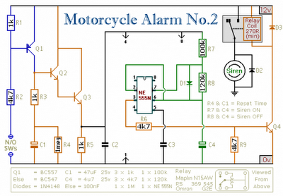
Any number of normally-open switches may be utilized. Install "tilt" switches that close when the steering is moved or when the bike is lifted off its side-stand or pushed forward off its centre-stand. Employ micro-switches to secure removable panels...
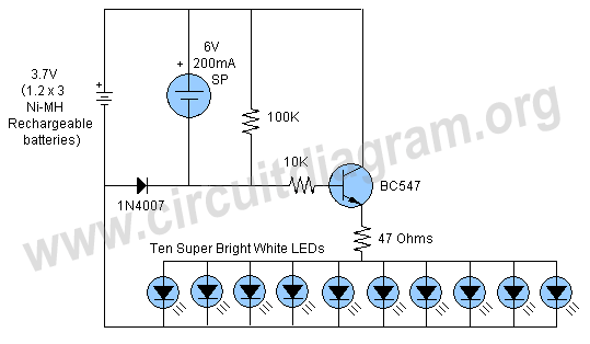
Schematic of an automatic solar garden light circuit with 10 super bright white LEDs that will automatically activate at night. The automatic solar garden light circuit is designed to harness solar energy for illumination purposes during nighttime. The circuit typically...
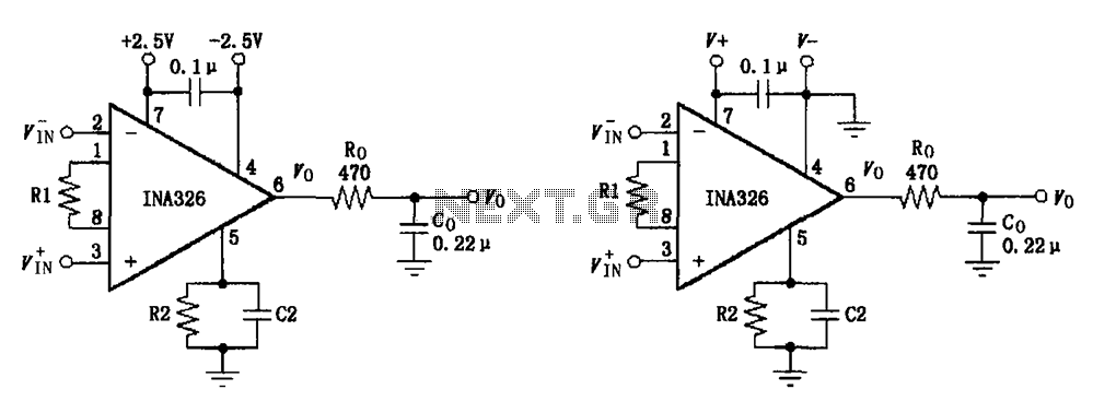
The basic connection circuit for the INA326/327 includes signals and power. A 0.1 µF capacitor is selected for power supply filtering and should be placed as close to the chip's supply pin as possible. Ro and Co serve as...
Warning: include(partials/cookie-banner.php): Failed to open stream: Permission denied in /var/www/html/nextgr/view-circuit.php on line 713
Warning: include(): Failed opening 'partials/cookie-banner.php' for inclusion (include_path='.:/usr/share/php') in /var/www/html/nextgr/view-circuit.php on line 713