
colpitts crystal oscillator circuit

The Crystal Colpitts oscillator is a popular choice in various electronic applications due to its stability and simplicity. The configuration primarily consists of a transistor, which serves as the active component, and a crystal that provides the necessary frequency stability. The use of a parallel mode crystal is critical, as it allows the circuit to leverage the crystal's resonance properties effectively.
In the schematic, the transistor is configured in a common-emitter arrangement, where the input signal is applied to the base terminal. The crystal is connected in parallel with the capacitors C2 and C3, which form a capacitive divider. This setup not only determines the oscillation frequency but also influences the overall gain of the circuit. The choice of the capacitors is crucial, as the ratio of C2 + C3 to C1 must be optimized to achieve the desired oscillation characteristics. A ratio of 5 to 10 to 1 is commonly employed to ensure a stable oscillation while minimizing loading effects on the crystal.
The capacitors C2 and C3 are selected to be of relatively high value, which helps to swamp out variations and drift that may arise from changes in transistor characteristics or temperature fluctuations. This design consideration is vital for maintaining the oscillator's performance over varying operating conditions. The capacitor C1, on the other hand, is used for fine-tuning the frequency of oscillation, allowing for precise adjustments to be made without significantly impacting the overall circuit stability.
The output of the oscillator is taken from the emitter of the transistor, where a clean sine wave can be observed. This output can be utilized in various applications, including signal generation, clock pulses for digital circuits, or as a reference frequency for other systems. Proper layout and component selection are essential to ensure that the oscillator operates efficiently and reliably, making the Crystal Colpitts oscillator a versatile and effective solution in electronic design.This is a design schematic of a Crystal Colpitts oscillator can be implemented using a transistor and a parallel mode crystal. This is the figure of the circuit. In this circuit, the crystal is use as an inductance. A large value capacitive divider is used between gate, source, and ground, and a small series capacitor is placed in the crystal circ
uit. You should choose the components values so that C2+C3 to C1 ratio has the highest possible value. The ratio of 5 to 10 to 1 is usually used. The schematic shows the typical values. This circuit introduce is a little loading on the crystal. The relatively high value is of C2 and C3 swamp out variations and drift caused by variations in device characteristics. Frequency can be fine tuned with C1. A clean enough sine wave appears at the emitter of the transistor. 🔗 External reference
Related Circuits

This circuit employs an HA-5152 dual operational amplifier and a field-effect transistor (FET) to create a low-voltage, low-power Wien bridge sine-wave oscillator. The frequency of oscillation is controlled by resistors and capacitors, while the FET functions as a voltage-controlled...
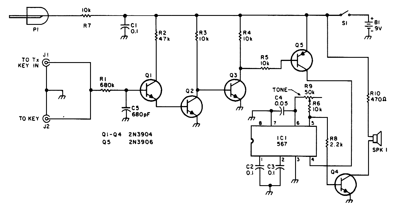
This circuit is designed for low-power transmitters that operate with a positive keying voltage. The transistors Q1, Q2, and Q3 are configured as a switching amplifier. When the key is pressed, the collector of Q3 connects to ground, which...
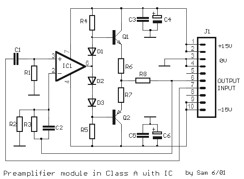
The circuit is based on a single operational amplifier integrated circuit designed to produce a modular preamplifier that operates in Class A configuration. The modular preamplifier circuit utilizes a single operational amplifier (op-amp) integrated circuit, which serves as the primary...

To initiate the timing process, there are two options available: either connect the START point to ground (GND), in which case the timer activates when connected to the voltage supply, or employ a switch to start the timer. The timing...
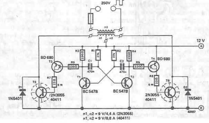
A simple portable converter that transforms 12V to 250V can be constructed using this circuit diagram. This converter is intended for portable use with a 12V car battery. A built astable multivibrator, consisting of transistors T1 and T2, generates...
This caller ID circuit utilizes the Motorola MG145447 IC chip. The service must be available from your local phone company for this circuit to function properly. The caller ID circuit based on the Motorola MG145447 IC chip is designed to...