
Combinatorial and Sequential Circuits
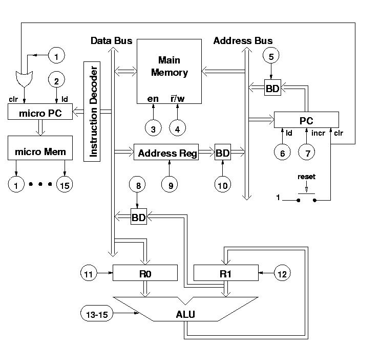
At the lower section of the diagram lies the arithmetic unit, which includes two general-purpose registers, R0 and R1. The loading of R0 from the data bus is determined by MOP 11, while MOP 12 controls whether R1 is loaded from the ALU's output. The ALU operations are managed by MOPs 13 to 15. The inputs to the ALU are 8 bits wide, sourced from registers R0 and R1, and the output, also 8 bits, is directed to R1. The output of R1 can be linked to the data bus through MOP 8, which interfaces with a bus driver (BD), effectively establishing a connection from R1's output to the data bus. The input to R1 is managed by MOP 4; when MOP 4 equals 1, memory writing occurs. The memory address is derived from the address bus, with data being output to the data bus during read operations or sourced from the data bus during write operations, making the memory data lines bidirectional.
In the central part of the diagram, an address register facilitates communication between the data bus and the address bus. It is loaded when MOP 9 equals 1, and its contents can be transmitted to the address bus through a bus driver controlled by MOP 10. This allows data from main memory or R1 to serve as addresses in main memory. The micro PC retains its value after the clock pulse if all inputs are 0. The value of the PC can be communicated to the data bus via a bus driver using MOP 5, which is the mechanism for fetching instructions for execution.
The micro memory is organized to ensure that address 0 contains the starting point of a micro program dedicated to fetching the instruction code located in the main memory address specified by the PC. Thus, to initiate the instruction fetch micro program, the PC must be directed to the next instruction for execution. Fetching an instruction requires only one clock cycle, necessitating the communication of the PC contents to the address bus via MOP 5 and reading from memory through MOP 3. The main memory contents at this address will be translated by the instruction decoder into the corresponding micro memory address where the micro program for the instruction is located. This address is then stored in the micro PC using MOP 2. Conventionally, the PC is incremented to ensure it points to the correct location for loading instruction arguments, or to the next instruction if none are present. Consistency in this convention is crucial.
The complete micro program for loading and decoding an instruction is now established, paving the way for the development of micro programs for individual instructions. The next steps involve detailing the specific micro programs corresponding to various instructions.To the left in the diagram, you find the micro memory containing up to 64 different addresses each with 15 bits (numbered 1 to 15) that we call the micro operations or MOPs for short. The MOPs control every aspect of the computer. To the left, you also find the micro PC, which is a counter register with clear. The width of the micro PC is 6 bits for a total of 64 different values. The micro PC is controlled by MOPs number 1 and 2. When MOP number 1 has the value 1, the micro PC will be cleared after the next clock pulse. Similarly, MOP number 2 will cause a new value to be loaded into the micro PC from the instruction decoder. The micro PC can also be cleared manually from the reset button. Since the The final item to the left of the data bus is the instruction decoder. Its job is to translate instruction codes to addresses in the micro memory where the micro program for the instruction starts.
The input to the instruction decoder is the low 5 bits of the data bus, and the output is 6 bits wide. The lower part of the diagram is the arithmetic unit with two general-purpose registers, R0 and R1. Whether R0 is loaded from the data bus is determined by MOP number 11. Whether R1 is loaded from the output of the ALU is controlled by MOP number 12. The ALU uses MOPS 13 to 15 to control what operation is to be performed. The inputs (8 bits wide) are taken from the registers R0 and R1 and the output (also 8 bits wide for now) goes to the input of R1.
The output of R1 can be connected to the data bus by MOP number 8 which is connected to a bus driver (BD) which in effect closes the connection from the output of R1 to the data bus. input is controlled by MOP number 4. When MOP number 4 has the value 1, the memory is written. The address of the memory is taken from the address bus and that date is output to the data bus (in the case of read) or taken from the data bus (in the case of write).
Thus the data lines of the memory are bidirectional. In the middle of the diagram, you find another register called the address register. It is used to communicate data from the data bus to the address bus. It is loaded whenever MOP number 9 has the value 1. The contents of the address register can be communicated to the address bus through a bus driver conrolled by MOP number 10. This way, data from main memory or from R1 can be used as addresses in main memory. are all 0, then PC retains its value after the clock pulse. The value of PC can be communicated to the data bus through a bus driver by MOP number 5. This is the way instructions are fetched for execution. Let us now study the contents of the micro memory. The micro memory is 15 bits wide, one bit for each MOP. We shall organize the micro memory so that address 0 always contains the beginning of a micro program to fetch the instruction code at the address in the main memory stored in PC.
Thus, when we start the instruction fetch micro program, we must make sure that PC points to the next instruction to execute. As it turns out, fetching an instruction only requires a single clock cycle. We need to communicate the contents of PC to the address bus using MOP number 5, we need to read from memory using MOP number 3.
The contents of the main memory at that address will be translated by the instruction decoder into the address in the micro memory where the micro program for the instruction starts. We need to store that address in micro PC using MOP number 2. Finally, by convention, we increment PC so that when a specific micro program needs to load instruction arguments, PC already points to the right place.
If the instruction has no arguments, then PC will simply point to the next instruction. We shall make sure we use this convention consistently. We now have the entire micro program for loading and decoding an instruction: We are now ready to atttack the micro programs for the individual instructions. The first instruction we shall 🔗 External reference
Related Circuits
This circuit employs a ring counter consisting of Q3, Q4, and Q5. Q2 functions as an oscillator that sequentially triggers the SCRs Q3, Q4, and Q5. When an SCR is activated, a 0.2 µF capacitor facilitates commutation, turning off...
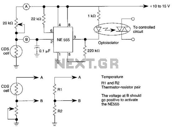
This dark-activated relay switch can be utilized to activate walkway or other outdoor lighting at dusk. By employing alternate connections to points A and B, it is capable of sensing varying levels of illumination, as well as high and...
The light fader circuits described here share a common concept of creating a gradual "cool" switch ON and switch OFF effect for connected lamps. This means that each time the lights are activated, the result is a smooth transition...
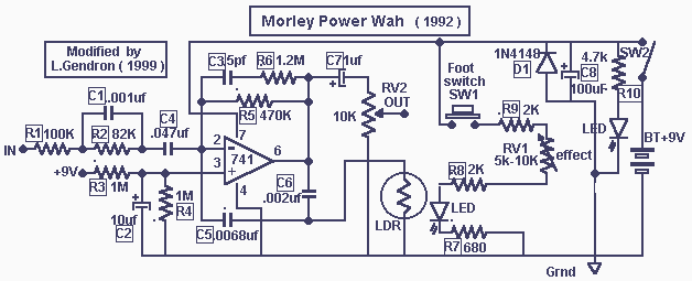
These two projects, Wah and Fuzz, are the results of a modification to a Morley dual channel volume control pedal that one of my sons suggested I undertake as he had no use for the volume unit but thought...
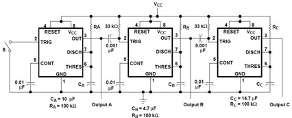
A sequential timer circuit device is utilized in various applications for initializing conditions during start-up or for activating test signals in sequences, such as in test equipment devices. The circuit diagram below illustrates a sequencer circuit with potential applications...
Commercial FM demodulation occurs at an intermediate frequency (IF) of 10.7 MHz. With a frequency deviation of ±75 kHz, the deviation of the IF carrier is approximately ±0.7%. This deviation allows for the conversion of FM to AM or...
Warning: include(partials/cookie-banner.php): Failed to open stream: Permission denied in /var/www/html/nextgr/view-circuit.php on line 713
Warning: include(): Failed opening 'partials/cookie-banner.php' for inclusion (include_path='.:/usr/share/php') in /var/www/html/nextgr/view-circuit.php on line 713