
Controllable integrator F007 schematic
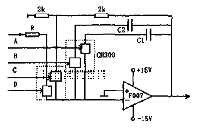
The controllable integrating circuit is designed to perform integration of input signals over specified time intervals, which can be adjusted according to the application requirements. The reset-to-zero feature allows the circuit to clear its output, ensuring that the integration process can start anew without residual effects from previous inputs. This is particularly useful in applications where precise timing and signal processing are critical.
The operational amplifiers F007 serve as the core components for signal amplification and integration. Their characteristics, such as gain bandwidth and input/output impedance, are essential for maintaining the integrity of the signals being processed. The integration time constant, determined by the resistor R and capacitors C1 and C2, can be tailored to suit the desired response time of the integrator. By configuring these components, different integration rates can be achieved, allowing for versatility in signal processing applications.
The circuit's functionality is further enhanced by the use of the analog switch C, which can be controlled through the states of terminals A, B, C, and D. Each combination of these control signals corresponds to a specific operational mode of the circuit, as detailed in the accompanying table. This feature allows for complex signal processing tasks to be executed with ease, enabling the circuit to adapt to various input conditions and processing requirements.
In summary, this controllable integrating circuit is a sophisticated design that leverages operational amplifiers and configurable components to deliver precise integration capabilities with the flexibility of multiple operational modes, making it suitable for a wide range of electronic applications. As shown in FIG controllable integrating circuit. The circuit has reset to zero, and to keep different integration time constant controllable integrator. The analog switch is C H300, operational amplifiers F007. Figure R and C1, C2 values can be configured. 4 different analog switch control circuit so that the state perform different functions. Relationship between control terminal A, B, C, D status and functions shown in the table.
Related Circuits
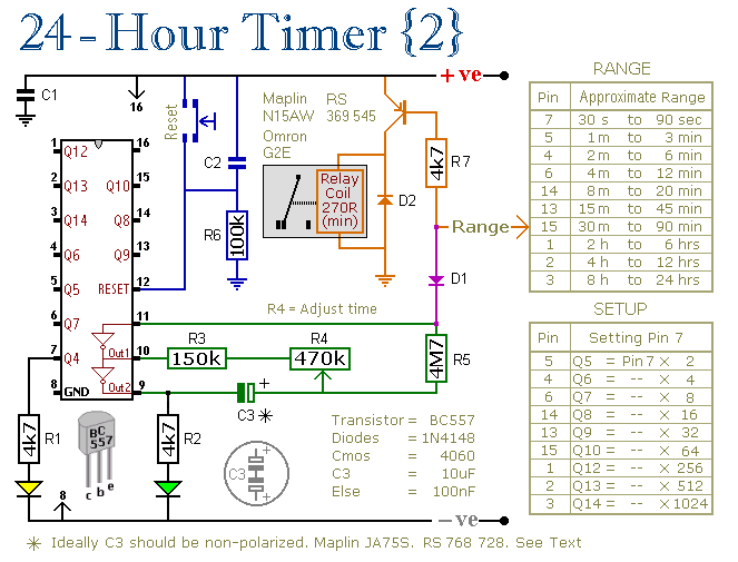
These two circuits are multi-range timers that offer periods of up to 24 hours and beyond. They can function as repeating timers or single-shot timers. Both circuits are fundamentally the same, with the primary distinction being their behavior in...
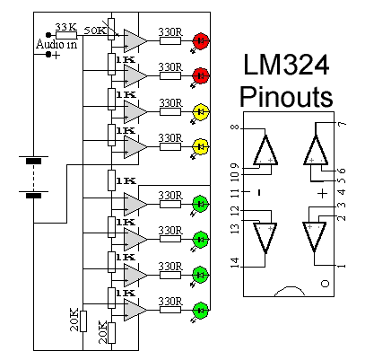
This circuit utilizes two quad op-amps to create an eight LED audio level meter. The op-amp employed in this circuit is the LM324, a widely used integrated circuit that is readily available from numerous electronic component suppliers. The 1K...
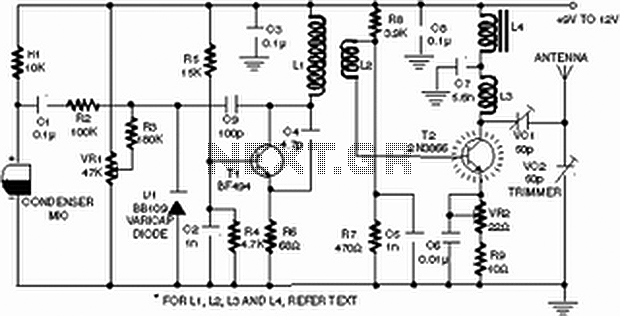
The power output of most of these circuits is very low because no power amplifier stages were incorporated. The transmitter circuit described here includes an additional RF power amplifier stage, following the oscillator stage, to increase the power output...
The low-cost integration circuit utilizes operational amplifiers as integrators; however, a CMOS inverter such as the CC4069 can also function as an integrator with favorable effectiveness at a low cost. The use of CMOS gates allows for an expanded...
Circuit IC1 provides a gain amplification of 40 dB, which decreases to approximately 20 dB when the frequency exceeds 500 Hz. To reduce resistor noise and the load on the operational amplifier at higher frequencies, the value of resistor...
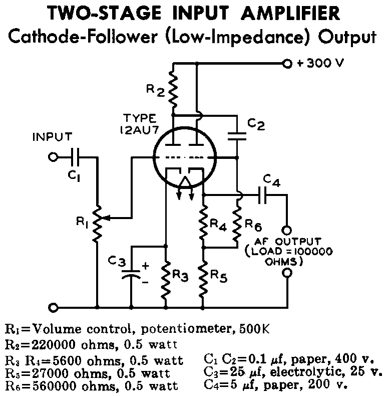
12AU7 (ECC82) Cathode Follower Tube Preamplifier Schematic. This is a two-stage 12AU7 preamplifier featuring a low impedance output stage. The overall gain is approximately 8 times. The 12AU7 (ECC82) tube is a dual triode commonly used in audio applications due...