
Counter Demodulates Narrowband FSK Without Synchronization

This noncoherent narrowband FSK receiver circuit offers several advantages over traditional designs that rely on PLLs or high-quality-factor filters. By eliminating the need for trimming adjustments and reducing sensitivity to noise, this circuit enables more robust performance in various applications. The use of resonant circuits for input filtering ensures that the desired frequency is effectively isolated, while the differential high-frequency amplifier provides sufficient gain to process the incoming signals accurately. The automatic gain control ensures that the output remains within a usable range, regardless of variations in signal strength. The digital conversion stage enables seamless integration with digital processing systems, allowing for efficient data handling and manipulation. Overall, this FSK demodulation circuit represents a significant advancement in the design of narrowband receivers, making it suitable for a wide range of modern communication systems.Frequency shift keying (FSK) is a popular digital modulation technique for data transmission. Some common applications of FSK modulation include both wired and wireless data transmission as well as infrared remote controls for consumer electronic equipment. FSK demodulation can be either coherent or noncoherent. Coherent detection always demands carrier and bit synchronization, typically achieved using phase-locked loops (PLLs).
PLLs are very noise-sensitive and normally call for a trimming adjustment inside the loop filter. FSK noncoherent demodulation can be implemented with two bandpass filters and two envelope detectors. Bit synchronization may be required as well. In narrowband FSK transmission systems, bandpass filters must have a very high quality factor, making implementation more complex.
This idea presents a noncoherent, narrowband FSK receiver that eliminates the drawbacks mentioned above. Figure 1 shows the FSK demodulation circuitry in which neither PLLs nor high-quality-factor bandpass filters are used.
With this high-frequency (HF) demodulation circuit, no trimming adjustments are necessary. L1, L2, C4, and C7 form two resonant circuits, implementing an input filter whose passband is centered at 10 MHz. A differential high-frequency amplifier amplifies the 10-MHz signal. IC1 and IC2 combine to make an automatic gain-control (AGC) circuit. The amplified signal is then converted into a digital waveform by a wideband comparator, IC3. The resulting digital signal clocks a 4-bit counter (IC4). Oscillator IC5 clears the counter. IC6A, the D-type flip-flop, latches the counter`s most significant bit at the rising edge of the oscillator signal OSC_OUT.
Since the oscillator circuit generates a 50% digital waveform duty cycle and the two FSK frequencies are: The calculated OSC_OUT frequency also can be divided or multiplied by a power of two. Counter IC4 counts only during the low period of the oscillation cycle. To clear the counter, the OSC_OUT signal`s remaining high period is used. IC5 can be implemented using a crystal oscillator module, a TLC555 in an astable configuration, or an oscillator circuit powered by a quartz crystal and a 74HCT02 IC.
Resistors R10 and R11 should have values equal to the HF_IN source impedance. For instance, if this FSK receiver is connected to a 50- © cable, then R10 and R11 should be 50- © resistors. This selection will provide maximum power transfer. Once diode D1 rectifies amplifier IC1`s output voltage, the resulting dc voltage is amplified and inverted by IC2A.
Differential amplifier IC2B inverts IC2A`s output voltage, producing a positive AGC voltage signal. IC2B also adds the REF voltage, which is scaled by resistors R1 and R4. The differential voltage amplification is then equal to 40 + 25(VREF ’VAGC), with VREF = 1. 4 V. IC3 receives the AGC-system output signal and converts it into a TTL-compatible signal to drive the IC4 clock. 🔗 External reference
Related Circuits

Shift pulses are generated by the unijunction transistors. The intervals between pulses are controlled by CT and RT. A different RT can be selected for each stage of the counter as shown. The circuit utilizes unijunction transistors (UJTs) to generate...
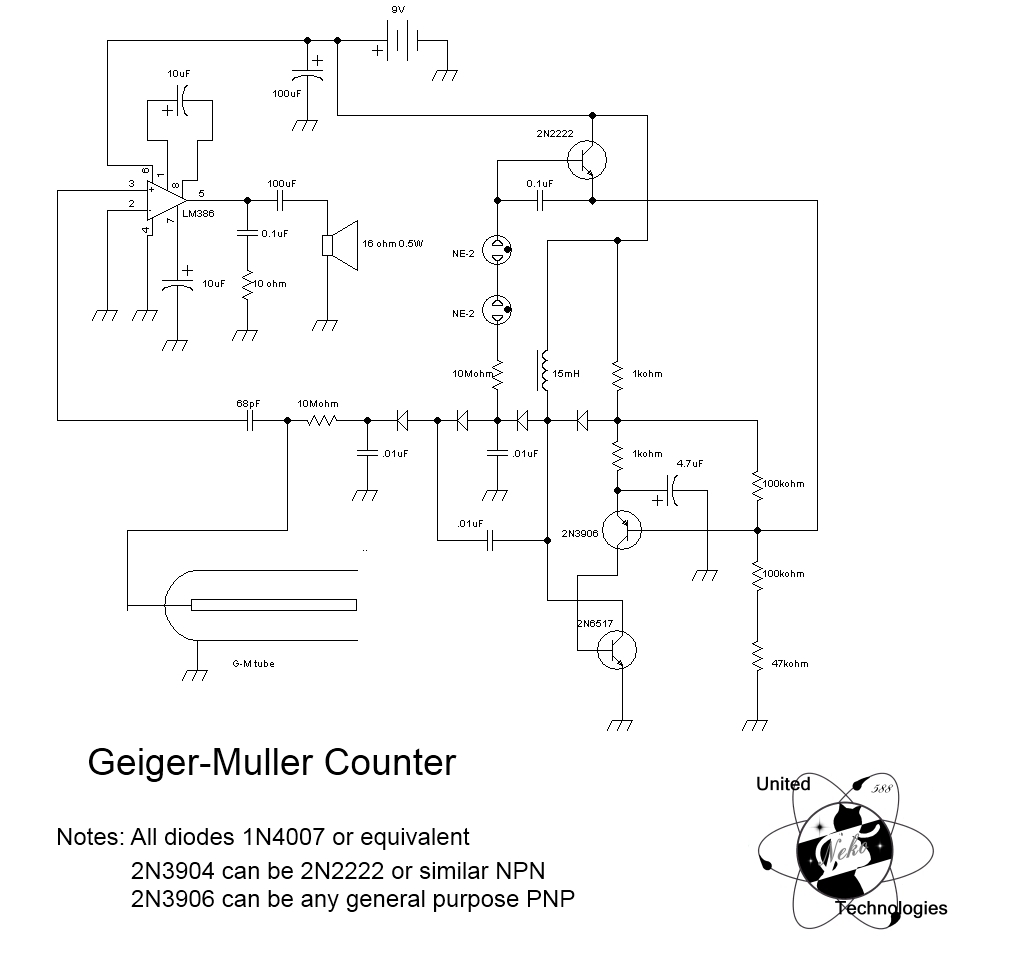
The basic charging circuit generates over 500V, depending on the inductor, component leakage, and other factors. The current output is limited by a 10 MΩ resistor, maintaining a short-circuit current under approximately 60 µA, making this project relatively safe....
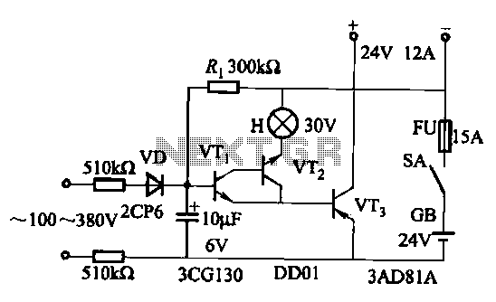
An AC-DC power supply without a power switching circuit is typically employed in lighting load circuits. When the power grid is restored, the standby power supply automatically switches on. The automatic switching circuit utilizes a transistor, as illustrated. The...
This simple counter can be used to count pulses, serving as the basis for a customer counter, similar to those found at the entrances of some stores, or for any other application requiring counting. The described simple counter circuit is...
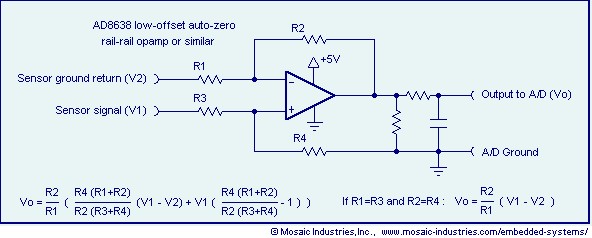
Ground loop offset errors and ground noise are eliminated by a differential amplifier or instrumentation amplifier before the analog-to-digital (A/D) conversion. The differential input amplifier addresses ground loop errors, allowing for precise measurement of non-isolated sensors. A simple operational...
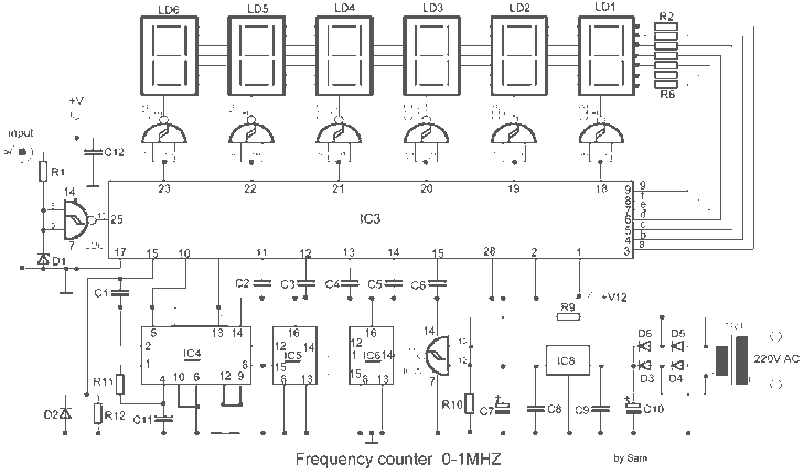
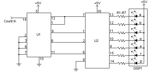
The MK50398 is one modern decimal counter up/down of six tens, with control of screen LED of seven segments and flip-flop of storage. Counter it can measure additive and abstractively. The IC MK50398 is ideal for manufacture frequency counter...