
CPLD Programming
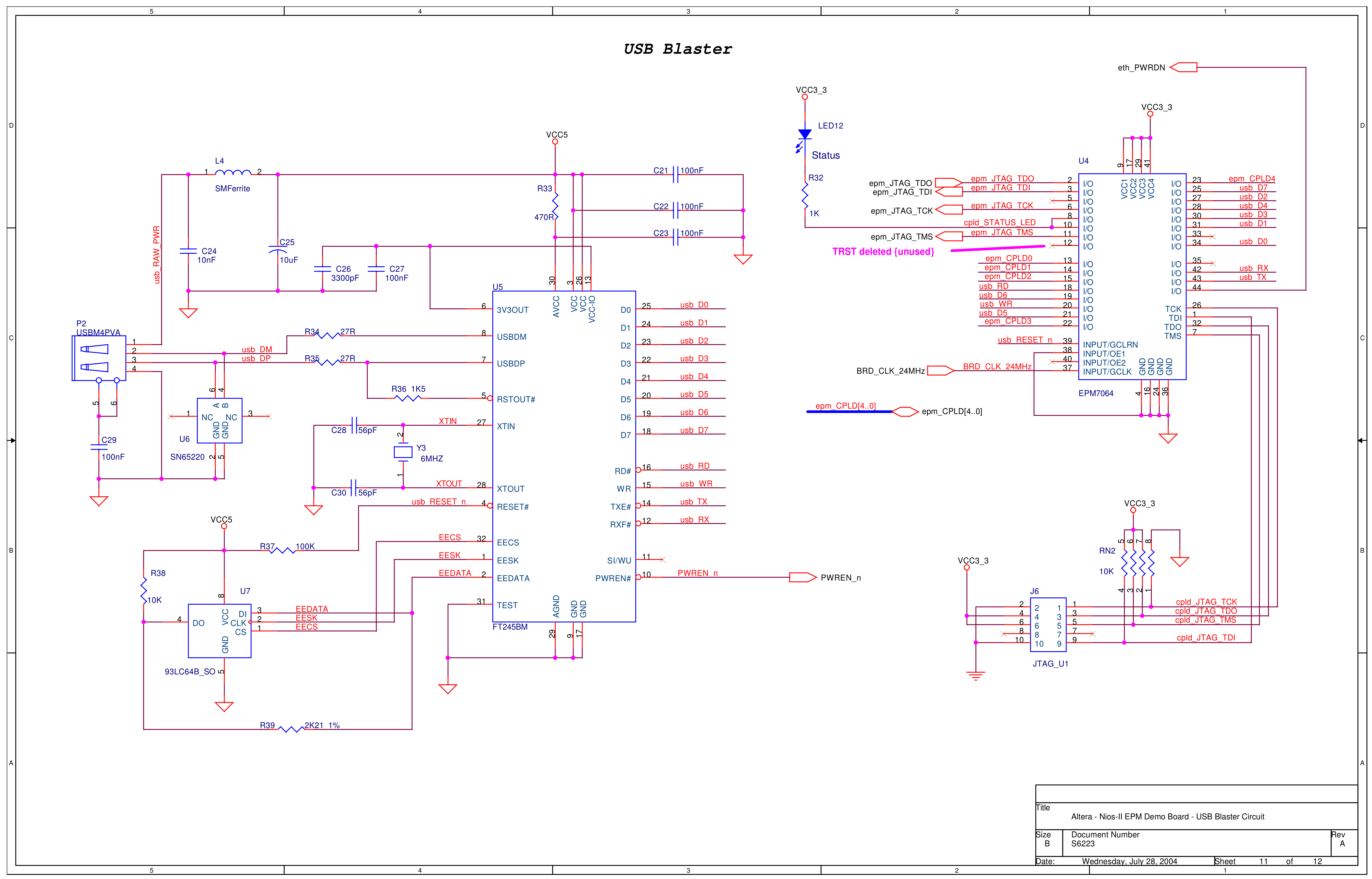
The programming interface circuit serves as a critical component for interfacing with FPGA and CPLD devices, facilitating the transfer of programming data through a straightforward connection method. The 10-pin interface, although primarily utilizing a few signal pins, establishes a reliable communication pathway between the programming device and the target chip. The JTAG interface is widely adopted in the industry due to its versatility, allowing for in-system programming, debugging, and testing of digital devices.
In practice, the connection of the USB-Blaster to the target chip involves careful attention to pin assignments, ensuring that the correct JTAG pins are utilized for programming. The integration of power supply connections (VCC and GND) is equally crucial, as proper power levels must be maintained during the programming process to prevent device damage or programming failures.
The ability to program various CPLDs and FPGAs through this interface not only enhances design flexibility but also promotes rapid prototyping and development. The evolution of JTAG programming methods, including the introduction of Active Serial and Passive Serial modes, further expands the range of devices that can be programmed, catering to different application requirements.
Overall, the implementation of a JTAG programming interface, such as the Altera USB-Blaster, represents a significant advancement in electronic design automation, enabling engineers and developers to efficiently program and debug complex digital systems. The accompanying standards and protocols established by organizations like IEEE ensure consistency and reliability across various programming applications, fostering innovation within the field of electronics.This Programming interface circuit sends the programming signals from the USB cable to the FPGA chip directly, through a standardized 10-PIN interface. Technically there are only 4 or 5 signal pins used, excluding GND and unused interface pins from the 10-PIN Ribbon cable that is commonly used by JTAG controllers.
Almost all FPGA and CPLD components have a set of devoted pins on the chip for this JTAG "In-System-Programming" interface. Here below is an older Altera MAX7000S CPLD chip which supports this JTAG interface used for special applications including a feature called "ISP" or In-System-Programming.
I have highlighted the JTAG interface pins in Yellow for your convenience. So all that is needed in order to program this chip, is to connect these JTAG pins from the chip to a USB-Blaster circuit. You then also connect all of the chips VCC and GND pins to source power and. The USB-Blaster or "JTAG" programming circuit is also available as an external JTAG controller called the "ALTERA USB-Blaster" as seen in the images below.
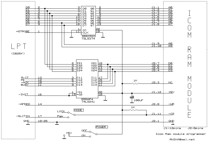
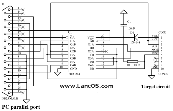
There was an older version of this JTAG controller called the Altera "BYTE-BLASTER-II" and it connected to your PC`s 25pin Parallel printer port. Having this "USB-BLASTER" JTAG controller gives you the option to program other CPLD`s and FPGA`s that provide the JTAG interface and support the "ISP" (In-Service-Programming) feature.
In turn, you can build your own PCB`s and program an Altera CPLD or FPGA device with your own logic design. The chip is programmed the same way you program your Altera development board through Quartus or your logic Synthesis software of choice.
Many of the older Altera CPLD chips require a special Master Programming unit, in order to be programmed and do not support the JTAG interface at all. The reverse is also true, for instance the Altera MAX II family of chips can only be programmed via a JTAG interface.
Most educational Development boards will have the JTAG port available for programming your target device, or it may be built right into the development board itself and all you need to do is connect a USB cable to commence programming. Now if you are etching your own PCB`s, you can build your own ISP programming interface using a JTAG programming device; such as the Altera "USB-BLASTER" or the "ByteBlaster II".
These Altera USB JTAG controllers vary in price, but are commonly available between $10. 00 & 30. 00 US dollars depending on the distributer. They are available from Amazon from the link below: This will allow you to build your own custom circuits & program various logic devices as shown in the photos below. You could also integrate a 10-pin programming port on your own PCB design to connect the USB-Blaster`s IDC ribbon cable to integrate JTAG ISP programming to your projects.
The Altera USB-Blaster is also able to program special Altera serial devices In-System, using two other programming modes known as the "AS" Mode (Active Serial) and "PS" Mode (Passive serial). You can use the chart below for the proper Pin connections for these Altera serial programming Modes.
After further development the "Join Test Action Group" found that the JTAG controller could be used for a number of different applications such as device programming. They decided to assign development teams to each of the various applications that the JTAG controller could be used for.
Once perfected they Standardized each group as an IEEE standard. IEEE 1532 = (ISP) An enhancement to 1149 🔗 External reference
Related Circuits
Everything appeared to be functioning normally. The half-duplex operation and pedal control in telegraphic mode allowed the operator to transmit while listening during pauses, seamlessly switching to the standard mode by simply pressing the pedal at the right moment....
A cellphone-operated robot is being developed, and there are challenges with programming the Atmega32A microcontroller. The recommended software for this task is AVR Studio 4. Within the Tools menu, the option "Program the AVR" can be selected, allowing the...
The Arduino Uno is a simple modification that bypasses the USB circuitry, allowing the device to be programmed using a serial port. The Arduino Uno is a widely used microcontroller board based on the ATmega328P microcontroller. It is designed to...
An 8x8-bit memory module was designed using LogicSim, a shareware software program that facilitates the creation of logic diagrams and the simulation of those designs. The memory module incorporates 688 logic gates and features multiple layers of abstraction to...
The Arduino system provides a straightforward and open-source approach for programming microcontrollers. Typically, this involves using a serial or USB cable directly connected to the microcontroller project. However, challenges arise when the project is located in inaccessible areas, such...
The delay timing setting of the program will depend on the CPU speed. The timing delay can be utilized from the C+ library, allowing the standard timing to be set on any computer, with a minimum achievable time delay...