
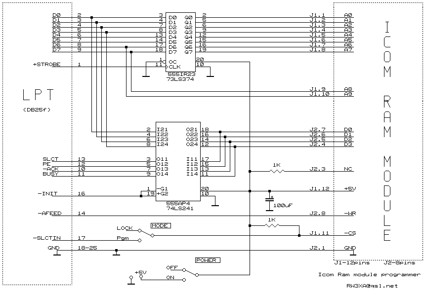
Icom IC-751 RAM reprogramming
The described circuit involves a half-duplex transceiver system that incorporates a pedal control mechanism for telegraphic operations. The system allows operators to transmit while simultaneously monitoring the output during pauses, enhancing communication efficiency. The transceiver's design features a dual-action control knob, which requires both pressing and turning to change frequency ranges. This design choice may lead to user frustration due to its complexity.
The unexpected frequency reading of 21049.4 kHz indicates a potential malfunction within the frequency selection circuitry. The reliance on CMOS technology for RAM storage introduces vulnerabilities, particularly in the event of power loss or component failure. CMOS ICs are known for their low power consumption but can exhibit erratic behavior when subjected to thermal stress or electrical overstress. The identification of a RAM module that retains critical operational data during power cycles is essential for maintaining the functionality of the transceiver.
The presence of a 3V lithium coin battery indicates a design consideration for non-volatile memory, allowing the device to retain settings and configurations even when powered down. However, the potential for failure in the CMOS RAM due to local breakdowns raises concerns about reliability. The process of unsoldering the battery to reset the RAM and restore normal operation is a practical solution, albeit one that may require technical expertise.
Overall, the described transceiver system showcases a blend of innovative design and inherent challenges associated with CMOS technology. The ability to troubleshoot and rectify issues related to memory retention and frequency selection is crucial for ensuring optimal performance in communication applications.Everything, it seemed, functioned normally. To me was pleased both half-duplex and work from the pedal in the telegraphic regime, when operator has the capability transferring, to listen to in the pauses of his transfer and here to pass into the usual regime, having simply harvested to the pedal at the necessary moment. Earlier I used the same approach with the construction of the home-made transverter, which worked with R -250M2.
Then I was switched to another band. To me was not immediately pleased used by designer sufficiently foolish ergonomics of double action, i. e. , pushing of knob, and then the turning of the tuning knob of apparatus for changing the range. However, I properly was worried, when, being located to 14025. 0 and changing range, I saw on the scale incomprehensible 21049. 4 kHz! Already having an experience with the transceivers, mentioned above, including the apparatuses of approximately the same class - 735 and 745, I was convinced that I must prove to be after the change of range to 21025, 28025 and so on.
But mysterious 049. 4 as before remained on the scale! I turned off transceiver, waited three minutes, then was again included it. Strange defect was present. Those of the readers, who although once read Murphy`s laws, must know that no one immediately reads instruction, encountering problems. Yes even Murphy`s itself recommends the reading them only when it ceases to work absolutely all. So I honestly continued further completely in accordance with old Murphy`s laws. Observing the strange transition point with the band selection, which by no means could not be explained from the position of the common sense (I he forgot about one - programmers in firm ICOM generally we could ever not be wireless enthusiasts), I solved, that some one of CMOS IS, which are been located inside, it was defective.
Before the fact in me was sufficiently "pleasant" long-term practice with Ukrainian CMOS IS of the production of Vinnitsa plant (well this trash, 4 to you I will report!), those with especially subjected to the effect of the fastening, when in IS occurs the local breakdown of CMOS- structures, it begins to consume high current, strongly it nagrevayetsya and it does not function, in full or in part, as it is assumed to it. I opened schematic diagrams, very rapidly revealed small RAM on the pay of processor even it defined, that IS RAM was executed exactly on the CMOS- technology (analog of our K537RU14, which can be here used).
Since RAM was energy-dependent, on the shawl was present small 3 v lithium small battery with size coin, preserving contained IS during turning offs of nourishment. 4 he already knew that turning off of nourishment with defective CMOS IS must end the begun effect of fastening and at the same time clean contained IS.
Certainly, I was confident, that in RAM must remain only the frequencies of the channels of memory and other current information of processor (stack, register records) - exactly as in those transceivers, with which 4 already dealt. Therefore 4 completely it did not fear, what these data propadut - you will think, will introduce the channels of memory again.
I boldly it took out to shawl RAM it unsoldered small battery by several minutes, sufficient, in order to unblock IS, which f 🔗 External reference
Related Circuits
The circuit consists of a 555 timer configured as an astable multivibrator along with resistors R1 and R2 and capacitor C1. It generates an oscillation frequency of approximately 10 kHz with a duty cycle close to 50%. Transistors VT2...

In an audio amplifier, the quality of sound depends on several factors, including the quality of active and passive components, circuit configuration, and layout. The selection of components is influenced by the constructor's budget. Discrete active components like transistors...
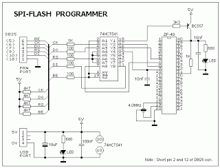
This ISP programmer can be utilized for in-system programming or as a standalone SPI programmer for Atmel ISP programmable devices. The programming interface is compatible with STK200 ISP programmer hardware, allowing users of STK200 to employ the software, which...
This project is based on the parametric equalizer proposed by Elektor in the late 1980s or early 1990s and later published in the book "Creations Electroniques" in 1993 (Publisher: Publitronic). Their design involved three stereo potentiometers per channel, resulting...
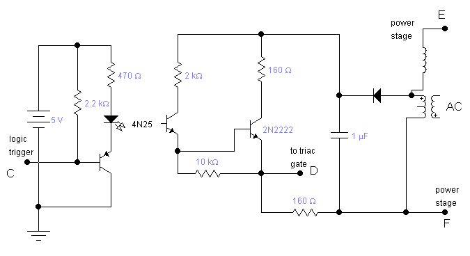
The circuit receives its input from the zero-crossing detector, which generates a 0-to-1-to-0 pulse to set the R-S flip-flop and activate the ramp circuit (A to Ramp) to initiate the timing ramp ascent. The described circuit operates by utilizing a...
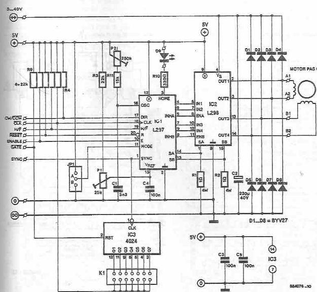
The L297 and L298 integrated circuits manufactured by SGS Thomson (ST) can be utilized to create a control circuit for a stepper motor, accommodating both two-phase bipolar and unipolar four-phase configurations, with a maximum current rating of 2 A...