
DDR memory power supply circuit

The DDR memory power supply circuit is designed to efficiently convert a variable DC battery voltage into a stable output voltage suitable for DDR memory operation. The MAX8632 chip serves as the core component of the power control circuit, managing the power supply by generating pulse-width modulation (PWM) signals. These PWM signals are crucial for controlling the switching action of the field effect transistors Q1 and Q2, which are configured in a push-pull arrangement.
The operation begins with the detection of the battery voltage, which can range from 4.5 V to 2.8 V. This range is essential for ensuring compatibility with various battery types and states of charge. The MAX8632 monitors this voltage and adjusts the PWM signals accordingly to maintain the desired output voltage. The switching voltage applied to the drain of Q1 allows for the modulation of the input battery voltage.
Transistors Q1 and Q2 are key components in this circuit, as they alternately conduct based on the PWM signals they receive. When Q1 is turned on, it allows current to flow from the battery through the load, while Q2 is turned off, and vice versa. This complementary operation ensures that the output voltage remains stable despite variations in the input voltage or load conditions.
The LC filter, composed of an inductor (L) and a capacitor (C), smooths the PWM output to produce a consistent 2.5 V output. This filtered voltage is crucial for the reliable operation of DDR memory, which requires a stable power supply to function correctly. The design of the LC filter is critical, as it must effectively reduce ripple voltage while maintaining efficiency.
Overall, this DDR memory power supply circuit exemplifies a robust design that efficiently converts battery voltage to a suitable level for memory applications, ensuring reliable performance in notebook devices.DDR memory power supply circuit Shows the notebook DDR memory power supply circuit, the power control circuit chip MAX8632, the chip power supply terminal VDD is Sv (detection point 1), the battery DC supply voltage between 4.5 V-2.8 V, the the switching voltage is applied to the field effect transistor Ql drain power supply control chip DH, DL outputs a PWM pulse of opposite phase signals, which signals are applied to Ql, Q2 of the gate, under the action of the PWM pulse Q1, Q2 alternately working, the DC voltage of the battery becomes switching voltage, and then after the LC filter output voltage of 2.V for the memory circuitry.
Related Circuits
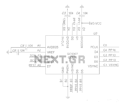
The system employs an optical fingerprint sensor utilizing the ARM Cortex M3 core, specifically the STMicroelectronics 32-bit high-performance microcontroller STM32F205RE. It incorporates a function body composition that utilizes the Sobel edge detection operator, Gabor filtering, image binarization, and various...
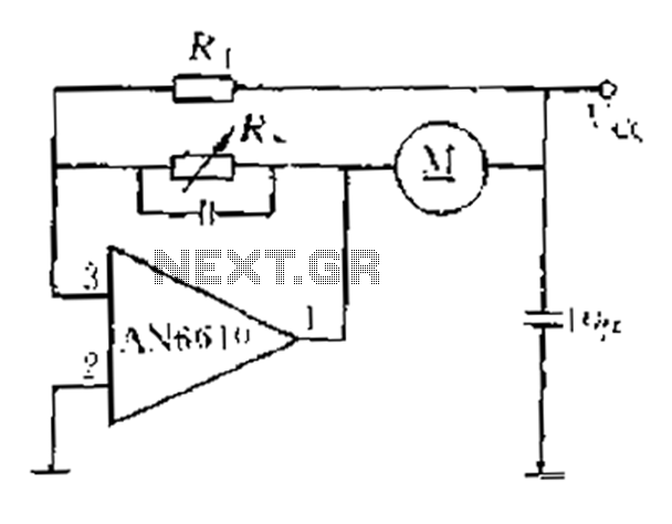
AN6610 Application Circuit operates as follows: When the supply voltage (Vcc) changes due to mechanical load variations, it can affect the motor speed. The motor speed is proportional to the back electromotive force (EMF). Consequently, the voltage across the...

This design circuit is for audio graphic equalizers, which are commonly found as commercial products, yet published circuits for them are quite rare. The circuit features a simple design that requires an operational amplifier (op-amp) to amplify the input...
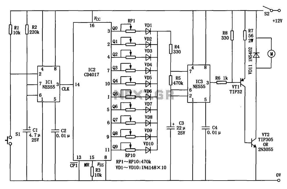
The circuit for a car wiper speed controller allows for adjustable wiper speed, ranging from one to ten cycles per second. This feature enables flexibility in operation and contributes to energy efficiency. The car wiper speed controller circuit typically employs...
If the audio input is a microphone, it is expected to precede an amplifier to achieve an output power of approximately 8W. The amateur seeking to enhance a small transmitter, which is likely already constructed, can utilize this circuit,...
This is a clap switch designed to avoid false triggering. To activate or deactivate any appliance, a user must clap twice. The circuit changes its output state only when two claps are detected within a specified time frame of...