
Decay mode input circuit

A resistor divider is a fundamental circuit configuration that utilizes two resistors to create a voltage output that is a fraction of the input voltage. This method is particularly useful in applications where signal levels must be adjusted to match the input requirements of subsequent stages in a circuit, such as in analog signal processing or interfacing with microcontrollers.
In a typical resistor divider setup, two resistors, R1 and R2, are connected in series across the input voltage (Vin). The output voltage (Vout) is taken from the junction between R1 and R2. The relationship between the input voltage and the output voltage can be expressed by the formula:
Vout = Vin * (R2 / (R1 + R2))
This equation illustrates that the output voltage is dependent on the ratio of the resistors. By selecting appropriate resistor values, the desired attenuation can be achieved. For example, if R1 is significantly larger than R2, the output voltage will be much lower than the input voltage, effectively attenuating the signal.
It is important to consider the impedance of the load connected to the output when designing a resistor divider. The load can affect the voltage division ratio, leading to inaccuracies in the expected output voltage. Therefore, the output impedance of the divider should be kept low relative to the load impedance to minimize the impact of loading effects.
In practical applications, resistor dividers are often used in sensor interfacing, level shifting, and signal conditioning circuits. Careful selection of resistor values is crucial to ensure the circuit operates within the desired parameters and maintains signal integrity. Additionally, the power rating of the resistors must be considered to prevent overheating and ensure reliable operation over time.FIG resistor divider attenuation measured mold humble way signal for higher signal amplitude situation.
Related Circuits
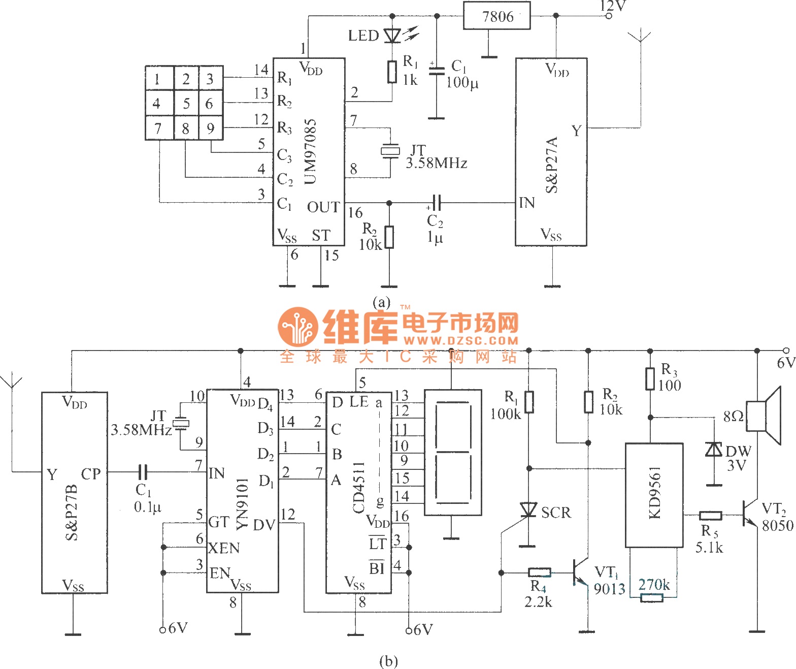
It utilizes a DTMF encoder output, which generates a dual-tone multi-frequency coded signal to modulate the transmitted carrier frequency. This configuration allows for the formation of a DTMF-encoded radio paging system. The circuit incorporates a DTMF encoding chip, UM97085,...
Figure 1-91 illustrates a practical loudness volume control circuit designed for integration with a preamplifier and tone control system. This circuit is positioned behind the output capacitor load (OCL) and can be connected to the main amplifier. Its effectiveness...
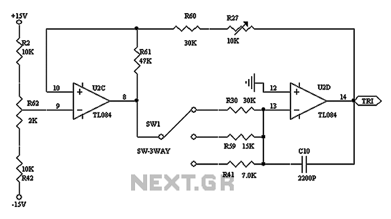
The triangular wave circuit consists of two operational amplifiers (OPs). R62 serves as the offset adjustment, while R27 is utilized for peak adjustment. A switch is included to select different resistances, allowing for the generation of triangular waves at...

A dimming circuit capacitor circuit is illustrated in Figure 2-63. When the switch SA is moved from position "1" to "3," the capacitance increases in ascending order, resulting in the light bulb brightness also increasing correspondingly. When SA is...
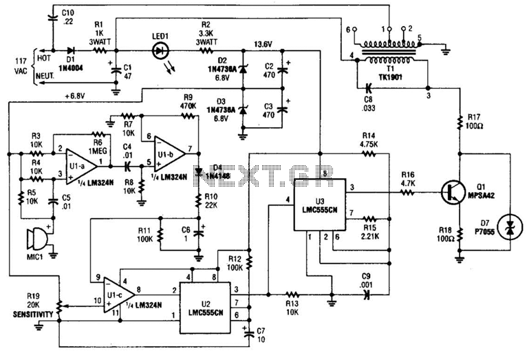
The baby-alert transmitter is constructed using an LM324 quad operational amplifier (U1), two LMC555CM CMOS oscillator/timers (U2 and U3), along with several supporting components. The transmitter activates upon detecting sound at MIC1, emitting a signal. Its operational frequency is...
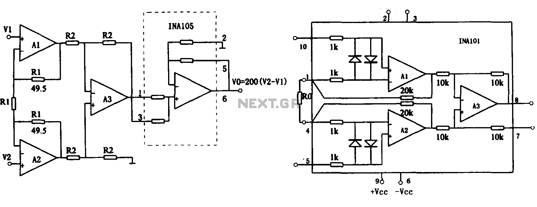
This document describes the extended common mode input voltage range of an instrument amplifier circuit. The circuit consists of three precision instrument amplifiers, A1, A2, and A3, which can be INA101 or INA102 models. The figure illustrates that A1,...