
Design Of Op Amp Sine Wave Oscillators
Designing a pulser with the HV732 involves utilizing the IC to create a basic high-voltage pulser for an ultrasound transmitter with a return-to-zero (RTZ) feature. The HV732 employs a capacitor-coupling circuit in its level translators, with the exception of the circuit driving the N-channel damping MOSFET, which is DC coupled. The design incorporates three 10 nF 200V ceramic capacitors (C6, C15, and C16) that serve to couple the driver output to the MOSFET's gate. The input stage of the HV732 is a high-speed level translator capable of operating with logic signals of 1.8V, 2.5V, or 3.3V. In this design example, the control logic signal is generated from an onboard Complex Programmable Logic Device (CPLD) chip, which operates at a logic level of 3.3V. The programmable CPLD utilizes an onboard 40 MHz crystal oscillator to produce a fast clock signal that controls the timing of the pulser. Additionally, there is a six-pin JTAG connection that facilitates convenient USB or parallel port programming of the CPLD from Xilinx.
The integration of these components allows for a robust and efficient ultrasound pulser design, suitable for various applications in medical imaging and testing. The HV732's high voltage capabilities, combined with its fast switching speeds, make it an ideal choice for driving piezoelectric transducers effectively. Proper attention to the design of the output stage and the selection of capacitors is crucial for achieving optimal performance and reliability in high-frequency applications.The HV732 is a complete, high-speed, high voltage ultra- sound transmitter pulser. This high performance CMOS in- tegrated circuit (IC) is in a single 7x7x0. 9mm 44-lead, multi- die, QFN package. The HV732 CAN deliver up to a ±2A source and sink cur- rent to the load transducer. It is designed to be used as a transmitter pulser in medical ultrasou nd imaging and ultra- sound material NDT applications. It CAN also be used for other piezoelectric or capacitive MEMS type transducers as a high voltage driver, or for ATE and pulse signal generators as a high voltage signal source. The HV732 has a built-in damping circuit to generate fast return-to-zero waveforms. It also has built-in, high voltage MOSFET gate-clamping functions to quickly change the out- put waveform amplitude.
HV732 circuitry consists of controller Logic circuits, level translators, a MOSFET driving Buffer gate-clamp circuits and MOSFET Transistors as the high current and high volt- age output stage. There are two pairs of MOSFETs in the output stage. Each pair is consists of a P-channel and an N-Channel MOSFET In each pair of MOSFETs the P-FET and N-FET are designed to have the same impedance and CAN provide peak currents of over 2 amps.
In the MOSFET gate-driver circuits, the output of the driver CAN swing from 0 to 12V on PDR and NDR pins, and the P-channel damping output swings from 0 to -5V on the DMPO pin. The HV732 CAN generate ±100V NRZ, RZ and PW pulses and low voltage CW waveforms. The up frequency limit of this IC is as high as 35 to 40MHz dependent on the load capacitance. Designing a Pulser with HV732 This application note describes how to use the HV732 to de- sign a basic high voltage pulser for an ultrasound transmitter with RTZ feature.
HV732 uses the capacitor-coupling circuit in its level trans- lators, except for the one driving the N-channel damping MOSFET which is DC coupled. There are three 10nF 200V ceramic capacitors, C6, C15 and C16, that provide the driver output to the MOSFET`s Gate coupling purpose.
The input stage of the HV732 is a high-speed Level Translator that is able to operate with Logic signals of 1. 8, 2. 5 or 3. 3V. In this design example, the control Logic signal is generated from an on-board CPLD chip. The Logic level of this CPLD is 3. 3V. The programmable CPLD uses an on-board 40MHz crystal Oscillator to generate a fast Clock signal to control the Timing of this pulser.
There is a six-pin JTAG connection for Xilinx`s convenient USB or parallel port CPLD programming link-cable. 🔗 External reference
Related Circuits

Up to 60 dB of gain at 455 kHz is available with the MC1350P. RES1 is a ceramic resonator, LC, or crystal filter. Keep the leads to pins 1, 2, 3, and 7 short. The MC1350P is a versatile integrated...
A broadband high-frequency amplifying circuit is primarily composed of a high-frequency matching transformer and an amplifying transistor. This circuit is designed to handle large high-frequency signals. The input of the amplifier circuit utilizes a matching transformer to ensure that...
The fins were added to a simple flat aluminium panel, and are made from 20 x 20 x 3mm aluminium angle. Their purpose is threefold - they improve the performance of the plate as a heatsink (although this is not...
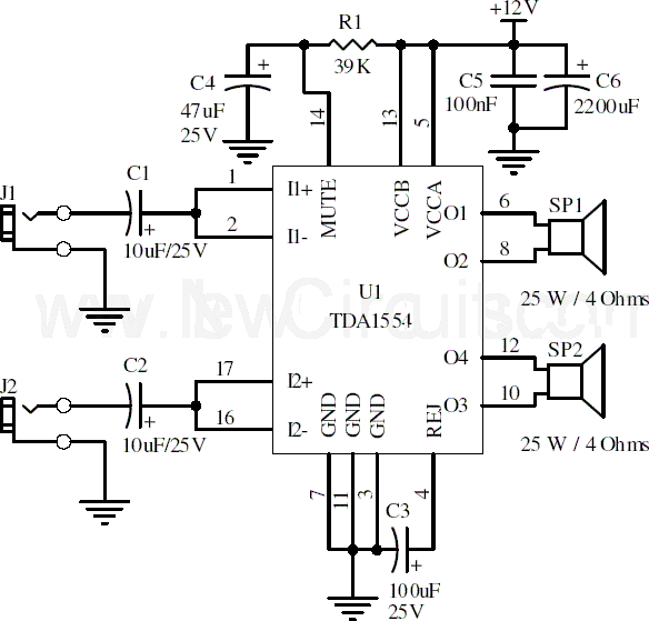
This document presents a 22-watt stereo audio power amplifier circuit diagram utilizing the TDA1554 integrated circuit from NXP Semiconductors (formerly Philips Semiconductors). The circuit is designed to effectively amplify stereo signals and is characterized by its simplicity and utility....
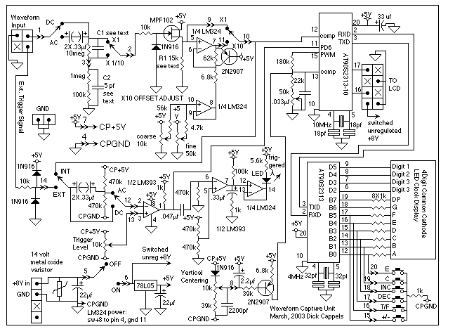
The result was a project that includes a waveform capture circuit, a graphic LCD (Liquid Crystal Display) and a control panel with LED indicators. As described, the display plugs directly into the waveform capture and control unit, which is...
Figure 3-25 illustrates a hybrid circuit featuring four input preamplifiers. The components C1, C2, C3, and C4 can accept signals from a microphone, line, phono, and crystal head respectively. The configuration allows for the individual or simultaneous entry of...