
Waveform Capture and Control
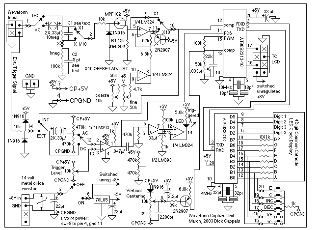
AC coupling through the two 0.33 µF capacitors in series gives a time constant on the input of about 2 seconds -may be a little long for some applications. The easiest way to shorten it is to replace the series capacitors (there are two of them because the ones in this range that I have on hand are tantalum) with a nonpolarized capacitor with a suitable voltage rating.
The 10:1 divider on the input circuit is frequency compensated with a single 5 pF capacitor to ground. If precision is required, metal oxide resistors can be used for a more stable divider, although this is only a 6-bit waveform monitor.
The ideal case when the divider switch is in the "X1/10" position is for the capacitance across the 10 MΩ resistor to be 1/10 the capacitance from the top of the 1 MΩ resistor to ground. A good practice is to place a relatively large resistor from the top of the 1 MΩ resistor to ground, say 10 or 15 pF, and then select or adjust a trimmer across the 10 MΩ resistor. This is analogous to how a X10 scope probe functions. If desired, the 10:1 divider can be omitted, grounding the bottom of the 1 MΩ resistor, running the top of the 1 MΩ directly to a BNC connector, and using it with either a X1 or X10 scope probe. An adjustment to the 5 pF capacitor may be necessary to ensure adequate shunt capacitance for frequency compensation.
The 10 kΩ resistor serves to limit current into the gate of the FET for large positive signals and to limit current into the 1N916 for large negative signals, thereby protecting the circuitry. However, there remains some susceptibility due to the shunt capacitance across the 10 kΩ resistor.
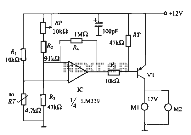
The FET in this circuit is an MPF102, although other JFETs may be suitable. The FET must be selected to provide a suitable shift in the DC level of the input signal when the input is grounded, ideally around 2.5 volts ± 1 volt. The LM324 operational amplifier operates from the unregulated power supply to provide additional latitude in this operating point. Care must be taken to keep the input level, which can exceed 1 volt P-P, well below 4.5 volts DC to maintain acceptable differential gain for 6-bit operation. The value of the 15 kΩ source follower resistor can be varied to obtain the necessary level shift, though larger values may adversely affect bandwidth, while smaller values could result in significant input signal loss.
A X10 direct coupled amplifier is implemented with an LM324, which has a gain-bandwidth product of 1 MHz. The 3 dB corner frequency of this X10 amplifier is approximately 100 kHz, a reasonable trade-off given the LM324's ability to operate from a single +5V power supply. The gain of the amplifier is determined by the 62 kΩ and 6.8 kΩ resistors, yielding a gain of about 10.1:1, which is only 1% off if the resistors are precisely valued. The feedback divider connects to a voltage follower made from another section of the LM324, which presents a virtual ground at approximately 2.5 volts, suitable given that the input signal was level shifted by the source follower. Input to the voltage follower is set by a coarse (10 kΩ pot) and a fine (50 kΩ pot) offset adjustment.The result was a project that includes a waveform capture circuit, a graphic LCD (Liquid Crystal Display) and a control panel with LED indicators. As described, the display plugs directly into the waveform capture and control unit, which is what the what the rest of this page is dedicated to.
The control panel controller appears as an ASCII terminal to the waveform capture controller and the two chips communicate using their on-chip hardware UARTs at 9600 baud. Both the controllers are Atmel AT90S2313. The control controller could have been implemented using an AT90S1200 but it was a little easier with the AT90S2313 because it has a hardware UART and a luxurious RAM stack, and by the time I came that part of the project I was much more anxious to see waveforms than to see if I could use the lower cost processor.
The board contains all of the analog circuit including the +5 volt power supply as well as the waveform sampling circuit and control panel interface with LED display. A clock display picked up surplus is used to display the sampling rate and it is driven by the control panel controller.
A separate LED mounted just below the clock display indicates that the sampling is being triggered and is driven directly by the analog circuitry. AC coupling through the two 0.33 uf capacitors in series gives a time constant on the input of about 2 seconds -may be a little long for some applications.
The easiest way to shorten it is to replace the series capacitors (there are two of them because the ones in this range that I have on hand are tantalum) with a nonpolarized capacitor with a suitable voltage rating. The 10: 1 divider on the input circuit is frequency compensated with a single 5 pf capacitor to ground.
I used parts I had on hand. If you are picky, you can use metal oxide resistors to get a more precise and stable divider, but remember this is only a 6 bit waveform monitor. The ideal case when the divider switch is in the "X1/10" position is for the capacitance across the 10 Meg Ohm resistor to be 1/10 the capacitance from the top of the 1 meg Ohm resistor to ground.
A good practice is to place a relatively large resistor from the top of the 1 meg resistor to ground, say 10 or 15 pf, and then select or adjust a trimmer across the 10 meg resistor. This is exactly how a X10 scope probe works, and if you are so inclined, you could skip the 10:1 divider, ground the bottom of the 1 meg resistor (short the 100k), run the top of the 1 meg straight to a BNC connector and use it with either a X1 or X10 scope probe.
If you do this you might have to increase the 5 pf capacitor a little bit to get a high enough shunt capacitance for the scope probe's frequency compensation to work. The 10k resistor serves to limit the current into the gate of the FET for large positive signals, and to limit the current into the 1N916 for large negative signals, thus protecting the circuitry.
There is still some susceptibility, however, because of the shunt capacitance across the 10k resistor, so don't go probing the output of a fluorescent LCD backlight with this. The FET in my circuit is an MPF102 but you can probably use any one of many JFETs you have around. The FET must be selected to provide a suitable shift in the DC level of the input signal when the input is grounded.
Try for 2.5 volts ± 1 volt, to allow some room for the signal. The LM324 operates from the unregulated power supply to provide a little extra latitude in this operating point, but remember to keep the input level, which can be 1 volt P-P or more plus the offset to well below 4.5 volts DC where the differential gain of the comparator on the AT90S2313 gets to be too poor even for 6 bit operation. The value of the 15k source follower resistor can also be varied to obtain the necessary level shift.
If the resistor gets too large, the bandwidth might suffer noticeably, and if it is made to small, then a lot of the input signal will be dropped across the source resistance, thought there is quite a bit of adjustment range in the waveform capture circuit itself to make up for quite a bit of this loss. A X10 direct coupled amplifier is implemented with an LM324. The LM324 has a gain-bandwidth product of 1 MHz, so the 3 db corner frequency of this X10 amplifier is 100 KHz, which is acceptable tradeoff given the LM342's ability to operate from a single +5V power supply and low cost.
The gain of the amplifier is set by the 62k and 6.8 k resistors. The gain comes out pretty close at 10.1:1, so it would only be 1% off if the resistors were right on value. The bottom of the feedback divider made of the 62k and 6.8k resistors connects to the voltage follower made from another section of the LM324, and this voltage follower appears as if it were a ground at about 2.5 volts, which is appropriate given that the input signal was level shifted up by 2.5 volts by the source follower.
The input to to the voltage follower is set by a coarse (10k pot) and a fine (50k pot) offset adjustment. 🔗 External reference
Related Circuits
PWM rectifier power controller power supply. Visit the page to read the explanation about the associated circuit diagram. A PWM (Pulse Width Modulation) rectifier power controller is a sophisticated electronic circuit designed to convert alternating current (AC) to direct current...
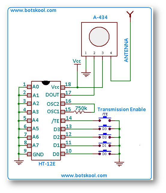
The following circuit illustrates an RF Remote Control Circuit Diagram. This circuit is based on the HT12E IC. Features include the original data in parallel format, where the decoder IC receives the signal through the RF receiver module, utilizing...

Manufacturer of thermoelectric materials, custom thermoelectric coolers, and value-added thermal assemblies. The manufacturer specializes in the development and production of thermoelectric materials, which are essential for converting temperature differences into electric voltage and vice versa. These materials are utilized in...
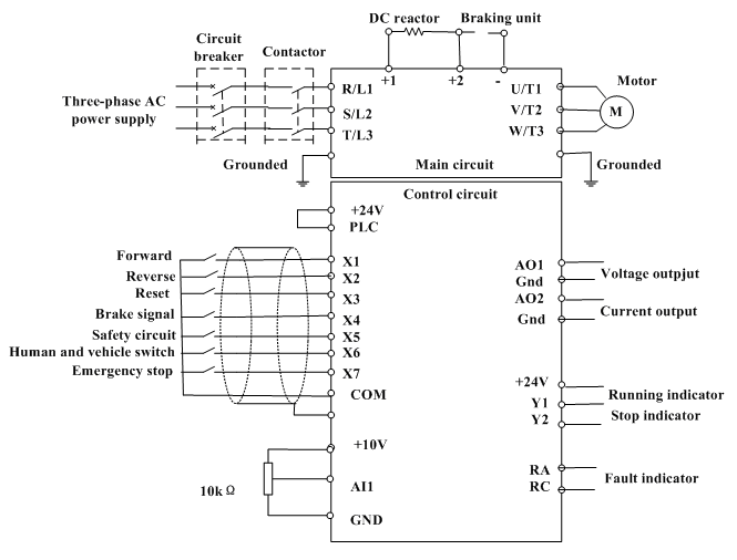
Motor control, energy efficiency of inverter (AC drive) selection, and parameters setting guidance in the mining industry: vector control, open loop or closed loop control, with energy braking unit or energy feedback unit. In the context of motor control for...
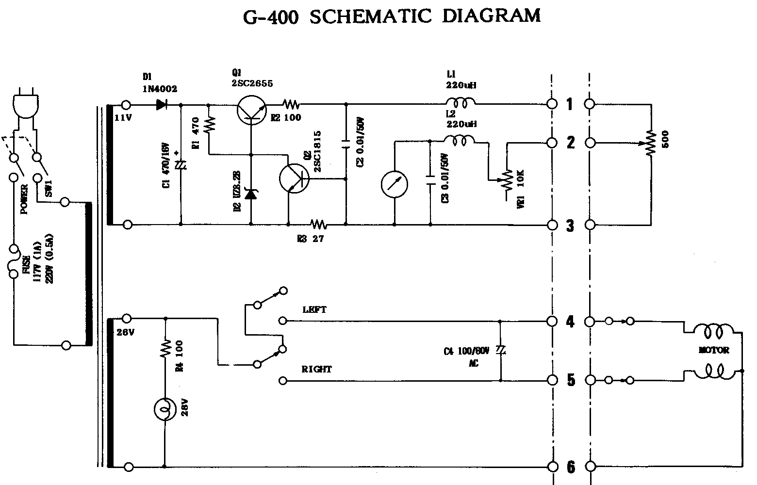
A very simple controller circuit with impressive performance. If a fully automatic computer-controlled rotator is not affordable but enhanced capability is desired from a basic rotator, the ZL1BPU Rotator Controller offers a simple "point and shoot" computer-controlled antenna solution....
When running large-scale software or games, a computer's internal temperature can increase significantly, especially during hot summer months. Although the machine is equipped with a CPU and graphics card fan, poor hot air circulation prevents immediate removal of heat...