
Device Switching Using Password

The heart of the transmitter section is the DTMF generator, which is implemented using IC1 (UM91214B). The entire transmitter is designed around this DTMF encoder IC. A crystal oscillator (XTAL1) is connected to pins 3 and 4 of IC1 to provide internal oscillation. The oscillated output is converted into a DTMF signal internally, producing a tone at pin 7 of IC1. The four rows of the keypad are connected to pins 15 to 18 of IC1, while the three columns are connected to pins 12 to 14, as illustrated in figure 2. Keys 1 through 9 control the device; key 0 is used to switch off the device, and key * resets the circuit. Key # is not utilized. A unique pair of sine waves, known as dual-tone multi-frequency (DTMF), is generated whenever a key is pressed on the keypad. The produced tones fall within the audible frequency range (300 to 2400 Hz) and are specifically chosen to minimize interference with normal speech. The tones consist of lower frequency rows (697 Hz, 770 Hz, 852 Hz, 941 Hz) and higher frequency columns (1209 Hz, 1336 Hz, 1477 Hz, or 1633 Hz), ensuring that none of the tones are harmonic with one another. The output tone from pin 7 of IC1 is connected to point A of the DTMF decoder circuit (IC2) as shown in figure 2.
The DTMF decoder utilizes the KT3170 IC, although the MT8870 can also be employed (IC2). A crystal oscillator is connected to pins 7 and 8 of IC2 to provide the necessary clock signal for the internal circuitry of the DTMF decoder. The binary output corresponding to the pressed key is obtained from pins 11 to 14 of IC2. When a key is pressed on the transmitter circuit, a valid DTMF tone is received by IC2, which decodes it into a 4-bit binary output. During the reception of the tone pair, the delayed steering output (StD) at pin 15 goes high, pulsing the clock pins of IC4 and IC5. The StD pulse is used to shift data in the dual 4-bit static shift registers of IC4 and IC5.
The password circuit is constructed using two dual 4-bit static registers (IC4 and IC5) and EX-OR gates (IC6 through IC9). EX-OR gates are utilized for cross-checking the entered password. The shift registers store the password in binary form. When a key is pressed on the keypad, a binary code from IC2 is fed into the shift register. Bits 1 to 4 are fed into IC4 (A), IC4 (B), IC5 (A), and IC5 (B), respectively. The shift registers receive a clock signal from IC2 through the StD pin 15 via an AND gate (N17). The decimal password is set using the keypad, with corresponding binary numbers fed through a DIP switch. The password set by the DIP switch, along with data stored in IC4 and IC5, should yield a low output across the outputs of IC11 through IC13. When the correct password is entered, the output of gate N22 goes low, as its inputs are connected to the outputs of gates N18 through N21, thus enabling the demultiplexer (IC3) and turning on the appliance. As illustrated in the circuit diagram, the output of gate N22 is connected to the input of AND gate N17, ensuring that the device functions as intended.Here is a project Device switching using password by innovative group Dreamlover technology, lets the user to lock their device with password. The block diagram of device switching using password is shown in figure 1. As the circuit device switching using password send as well as receive data it is divided into two main section i.
e. transmitter and receiver section (DTMF decoder and password setup section). Transmitter section: - The heart of the transmitter section (DTMF generator) is IC1 (UM91214B), the entire transmitter section is designed and fabricated around DTMF encoder IC (IC1). Cristal oscillator XTAL1 is used here for internal oscillation connected to pin 3 and 4 of IC1. The oscillated output is further converted into DTMF signal internally and as a result tone is obtained from pin 7 of IC1.
The 4 rows of keypad is connected to pin 15 to pin 18 of IC1, similarly 3 columns to pin 12 to pin 14 as shown in figure 2. Here, keys 1 through 9 is used to control the device, where key 0 is used to switch off the device and key * is used to reset the circuit.
The key # is not used here. A unique pair of sine wave [i. e. dual-tone multi frequency (DTMF)] is produced whenever any key of keypad is pressed. The produced is of audible frequency range (i. e. 300 to 2400 Hz) but is so chosen that the possibility of interface with normal speech simultaneously is minimized. The produced tone is pair of lower frequency rows (697 Hz, 770 Hz, 852 Hz, 941 Hz) and higher frequency columns (1209 Hz, 1336 Hz, 1477 Hz or 1633 Hz) in order to minimized the problem of interface.
We used here 11 unique combination of codes (tones) out of 16 allows by DTMF and are so chosen that none of the tones are harmonic in nature with each other. The output tone is available at pin 7 of IC1, connected to point A of DTMF decoder circuit (IC2) as shown in figure 2.
The DTMF decoder:- For DTMF decoder we use here DTMF decoder IC KT3170 but we can also use MT8870 (IC2). A crystal oscillator is connected to pin 7 and pin 8 of IC2 for providing necessary clock for internal circuit of DTMF decoder.
The binary output is obtained corresponding to the key pressed in the keypad of transmitter circuit. Whenever any key is pressed in transmitter circuit a valid DTMF tone is received by IC2 which further decoded into 4-bit binary output available at pin 11 to 14 which further decoded into 4-bit binary output available at pin 11 to 14 of IC2. At the time of receiving tone pair delayed steering output (StD) pin 15 goes high which further pulse the clock pin of IC4 and IC5.
Here, StD pulse is used to shift the data in dual 4-bit static shift register of IC4 and IC5. Password Circuit:- The password circuit is build and fabricated by two dual 4-bit static register(IC4 and IC5) and EX-OR ICs (IC6 through IC9). Cross-checking or for checking whether the entered password is correct or not EX-OR gate is used (IC6 through IC9).
The work of shift register is to store the password in binary form. When any key is pressed in keypad a binary code from IC2 is fed to shift register. Bit 1 to 4th bit is fed to shift register IC4 (A), IC4 (B), IC5 (A), IC5 (B) respectively. The shift register get clock from IC2 by StD pin 15 through AND gate N17. The decimal number password is set by keypad where corresponding binary number are fed through the DIP switch. The password set by DIP switch along with data stored in IC4 and IC5, should result into a low output across the output of IC11 through IC13.
The output of gate N22 goes low when correct password is entered because the input of gate N22 is connected to output of gate N18 through N21 which further enable the demultiplexer (IC3) and appliance is turned on. As from the circuit diagram the output of gate N22 is connected to input of AND gate N17. As a result whenever the o 🔗 External reference
Related Circuits
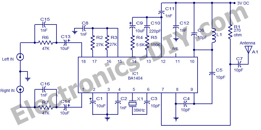
A high-quality stereo FM transmitter circuit is presented here. The circuit utilizes the IC BA1404 from ROHM Semiconductors. The BA1404 is a monolithic FM stereo modulator that incorporates a built-in stereo modulator, FM modulator, and RF amplifier circuitry. The...
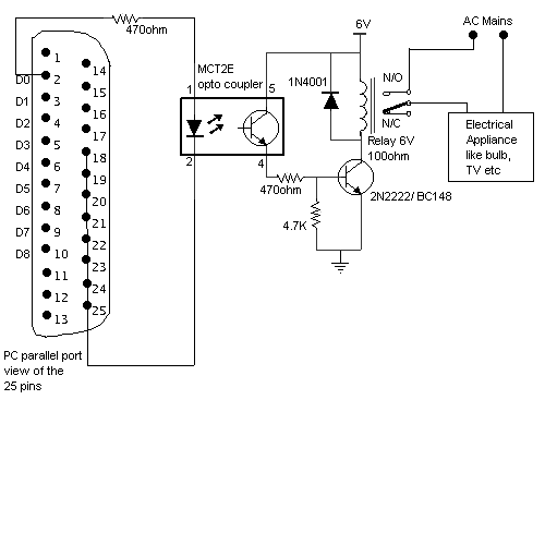
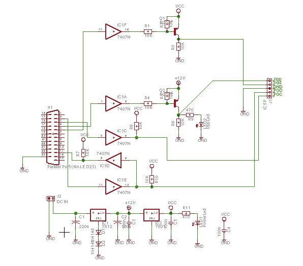
Control electrical appliances using a PC. This circuit utilizes the printer port of a PC for control applications through software and some interface hardware. The interface circuit is included. The described circuit leverages the parallel printer port (also known as...
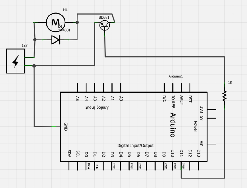
Power a 12V fan using a Darlington transistor to control the speed from an Arduino. When wired as described, nothing happens even though a PWM signal is being sent. It is suggested to edit the question and ensure the...
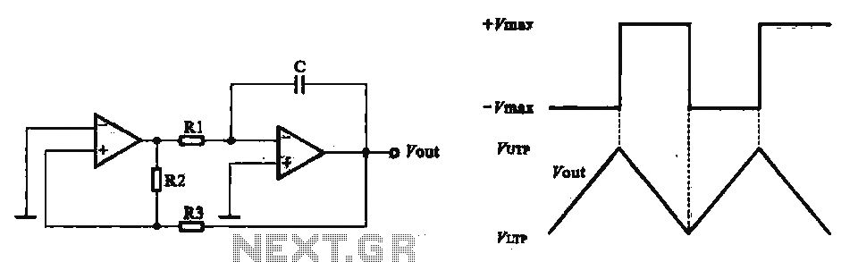
This circuit utilizes two operational amplifiers configured as triangular wave oscillators. It demonstrates a practical application of a relaxation oscillator that employs a voltage comparator to execute the switching function. The schematic in FIG. 2 illustrates the composition of...
Schaer is a generic programmer circuit capable of uploading and downloading firmware to and from several electronic devices, such as microcontrollers. The Schaer programmer circuit is designed to facilitate the transfer of firmware between a host computer and various electronic...
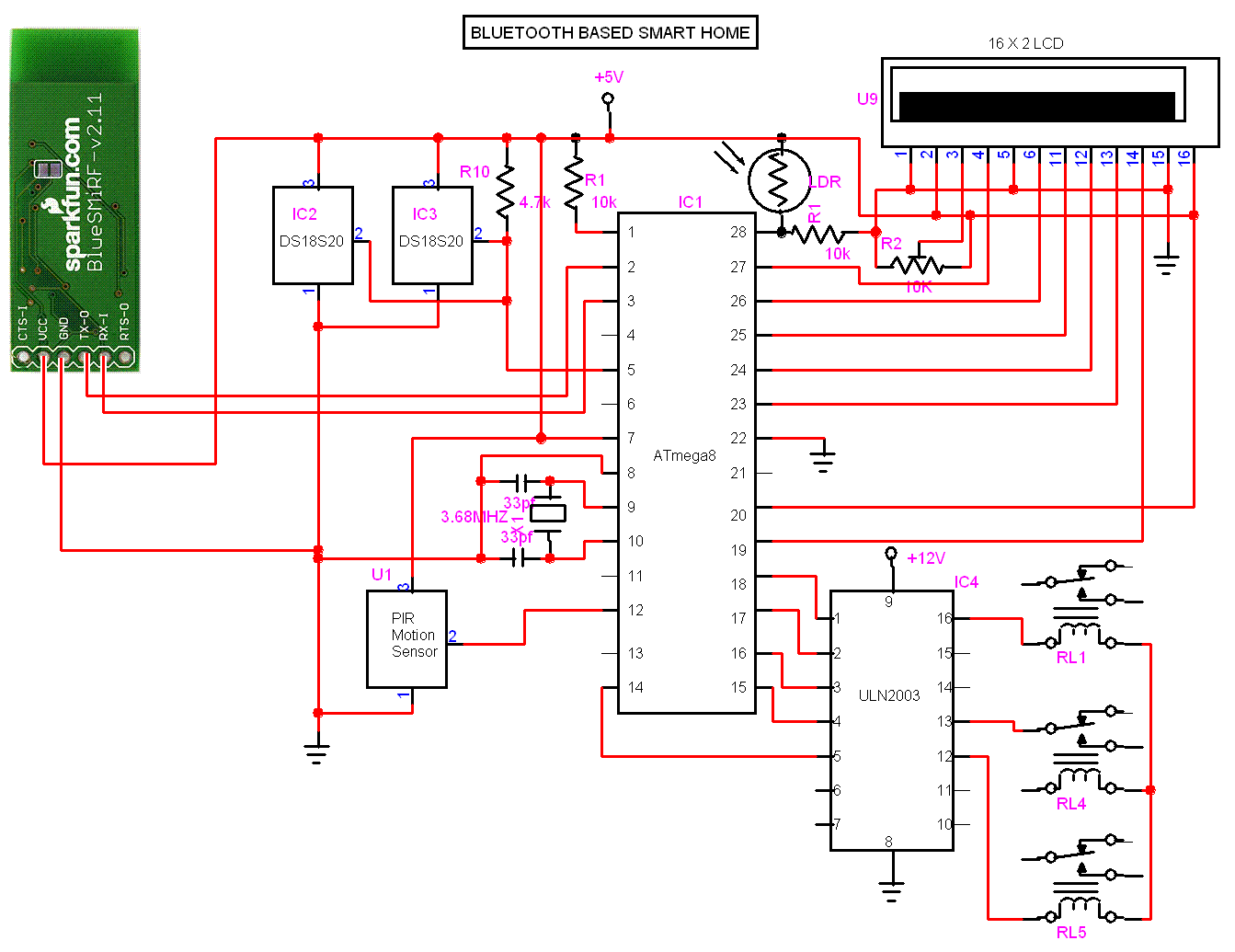
This project automates home appliances via a Bluetooth-enabled PC. A USB Bluetooth adapter is utilized on the PC side, while a Serial Bluetooth module is employed for communication. This project involves the integration of a Bluetooth-enabled PC with home appliances...