
digital clock
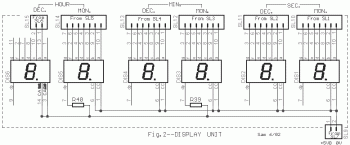
The digital clock circuit utilizes a combination of integrated circuits to manage timekeeping and display functions. The primary components include a microcontroller or timer IC, which serves as the core of the clock, along with additional ICs that handle the display and power management. The use of two distinct voltage lines, +5VA and +5VB, is crucial for the operation of this circuit. The +5VA line ensures that the majority of the circuit components are powered, while the +5VB line is specifically designated for the display and certain ICs, allowing for efficient power management.
In the event of a power failure, the circuit is designed to switch to battery operation, maintaining timekeeping functionality. This is achieved through a carefully designed power management system that disconnects the display from the main power supply while keeping the microcontroller operational. The incorporation of this feature is essential for ensuring that the clock remains functional even during power outages, thereby enhancing its reliability.
For PCB fabrication, the process begins with designing the layout in software such as Eagle, which provides tools for creating and modifying circuit schematics. Once the design is finalized, it can be printed onto photo or glossy paper using a laser printer, which is critical for achieving a high-quality transfer of the circuit pattern to the PCB. The printed design must then be adhered to the copper side of the PCB, followed by the application of heat using a hot iron. This step is crucial as it allows the ink to bond with the copper, creating a resist for the etching process.
After the design has been transferred, the PCB can be etched using a suitable etching solution, which removes the unprotected copper and leaves behind the desired circuit pattern. Once the etching is complete, the board can be drilled for component placement, and the components can be soldered in place to complete the assembly of the digital clock circuit. This methodical approach ensures that the final product is both functional and reliable, suitable for practical applications in timekeeping.This is digital clock schematic diagram. This circuit is quite complex and quite difficult for a newbie because this circuit uses IC with some a complicated connections. The voltages that supplied to the circuit are divided in two lines. The voltage +5VA supplies all IC except the IC9 until IC13 and is supplied with voltage in case of break of ne
twork voltage. On the other side, the voltage linr of +5VB only supplies the IC9 until IC13 and display and is interrupted in case of interruption of network voltage, it is to ensure the economy of battery. Make a PCB in very easy steps. ! Create your PCB design using PCB designer software like Eagle, print out your design on photo paper or glossy paper with laserjet printer.
Stick the printed design on the PCB (copper side) and then heat it using hot iron plate. The ink will stick on the PCB and it will be ready for etching process. Note: If you don`t have laserjet printer, then you can print the design on standard paper. Copy the printed design at Copy Service around your location (with glossy paper). 🔗 External reference
Related Circuits
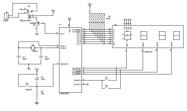
The circuit diagram above illustrates the Clock Controller V1.1. Pins P3.0 to P3.3 are connected to the base of a 4-PNP transistor, specifically the 2N2907, which is used to sink current. The Clock Controller V1.1 circuit is designed to manage...
Redesign a complex solution using minimal external components, resulting in a low-cost application that provides high-precision measurements. This digital thermometer microcontroller project utilizes a watchdog timer function to measure temperature. The watchdog timer (WDT) on all PIC microcontrollers has...
An analog electronic clock that utilizes a trigger signal for operation. An analog electronic clock typically employs a trigger signal to manage its timekeeping functions. The clock's primary components include a quartz crystal oscillator, which provides a stable frequency reference,...
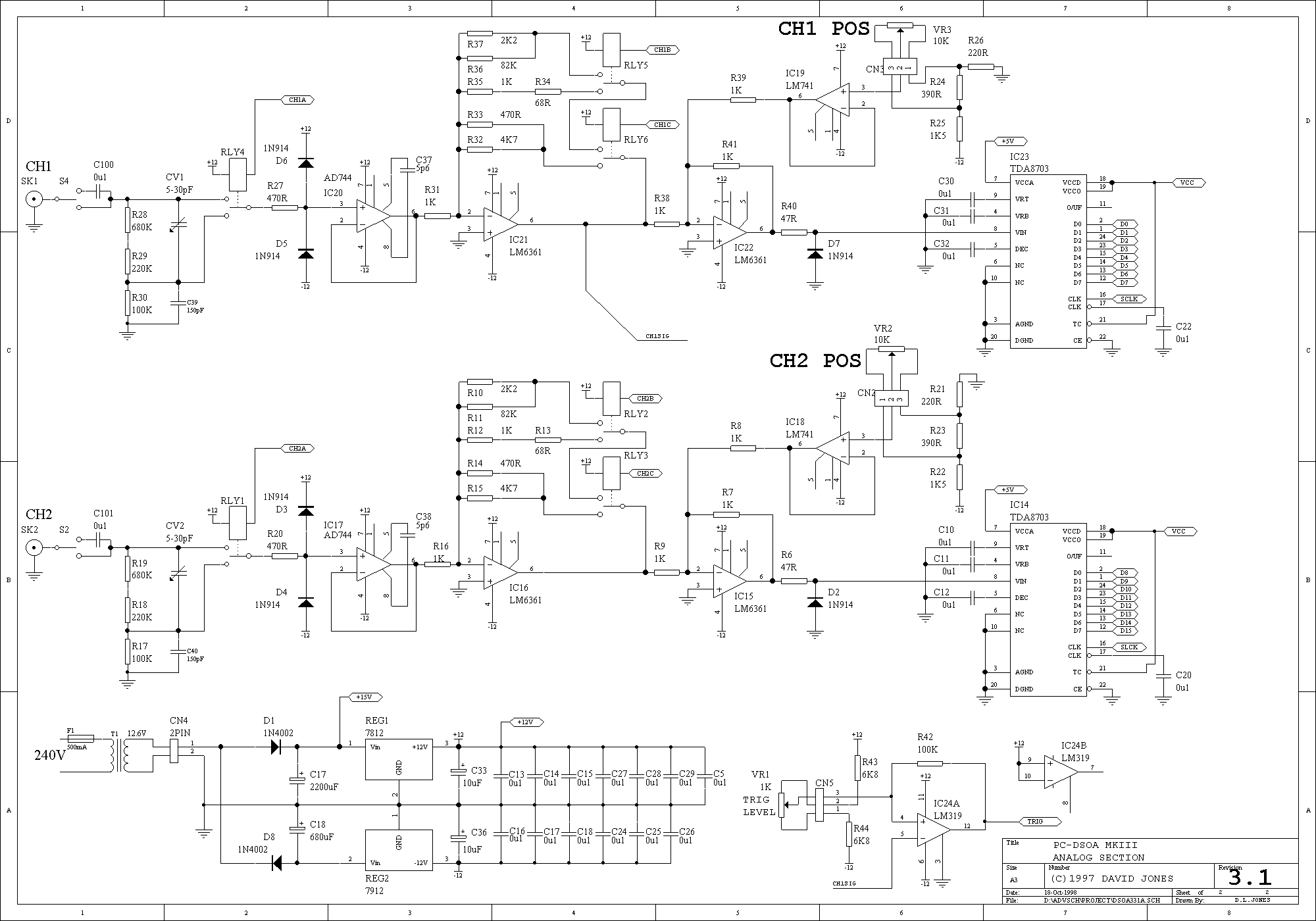
A follow up Mk2 version described by EA's Jim Rowe in the May/June/July 94 issues of EA improved on the original with calibrated time and vertical scales, and extra triggering features. This design proved even more popular than the...
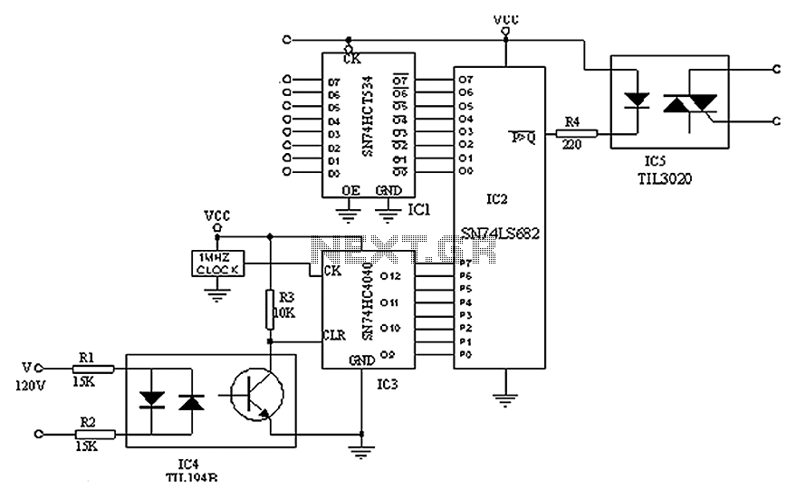
A simple digital circuit is presented that can be used to precisely control the AC power supply. This circuit does not include a digital-to-analog conversion component. In its application, effective control is established through a computer system that sends...
This document serves as a resource for developers who are new to Texas Instruments (TI) ARM-based processors, as well as for seasoned developers seeking to deepen their understanding of the different ARM architectures. It starts with an overview of...