
2n2907 For7-Segment Digital Clock Circuit
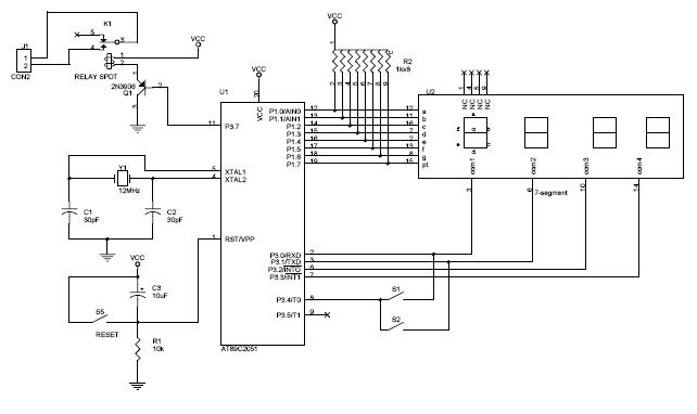
The Clock Controller V1.1 circuit is designed to manage timing and control functions in electronic applications. The primary component, the 2N2907 transistor, is a general-purpose PNP transistor capable of handling moderate currents, making it suitable for switching applications. The configuration of pins P3.0 to P3.3 indicates that these pins can be utilized as control signals to activate or deactivate the transistor, allowing it to sink current effectively.
In this setup, when a high signal is applied to any of the pins P3.0 to P3.3, the base of the PNP transistor becomes forward-biased, allowing current to flow from the collector to the emitter. This action enables the transistor to act as a switch, controlling the load connected to its collector. The load can be any device that requires a controlled power supply, such as an LED, motor, or relay.
The circuit may also include additional components such as resistors to limit the base current and protect the transistor from excessive current flow. A pull-up resistor may be employed to ensure that the transistor remains off when the control pins are not actively driven high. Furthermore, bypass capacitors could be integrated to filter any noise from the power supply, ensuring stable operation of the Clock Controller.
Overall, the Clock Controller V1.1 circuit provides a versatile solution for timing and control in various electronic systems, leveraging the capabilities of the 2N2907 transistor to manage current flow based on the signals from the microcontroller or other digital logic devices.Circuit above shows a circuit diagram of the Clock Controller V1.1. P3.0-P3.3 also drives a base pin of 4-PNP transistor, 2n2907 with sink current .. 🔗 External reference
Related Circuits
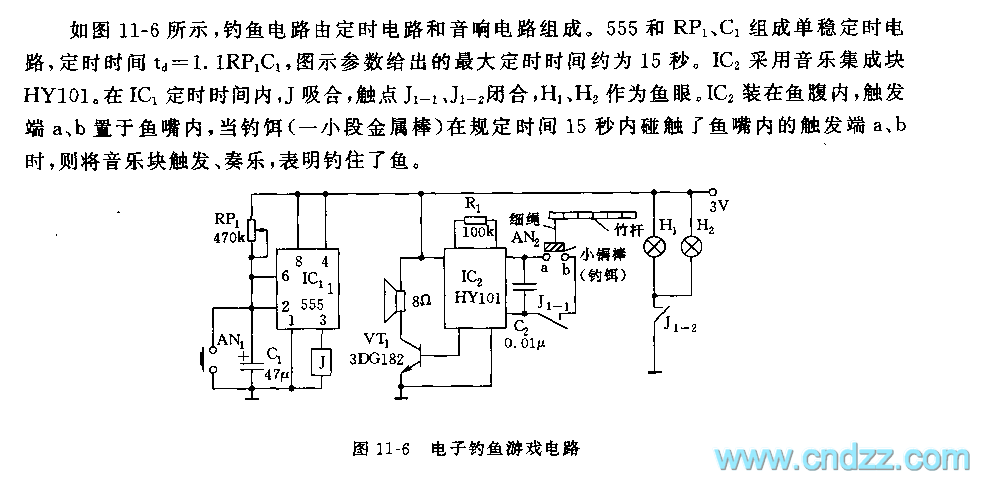
The fishing circuit, as illustrated in figure 11-6, comprises a timing circuit and an audio circuit. The components 555, RP1, and C1 form the single-shot circuit, with the defined time calculated as td = 1.1RP1C1. The maximum defined time...
The circuit for the RS232 serial interface exhibits mild complexity. The primary components of the circuit include the 18F4520 microcontroller, MAX233A level shifter, and a DB-9 connector. This circuit utilizes a basic +5V power regulator to supply the digital...
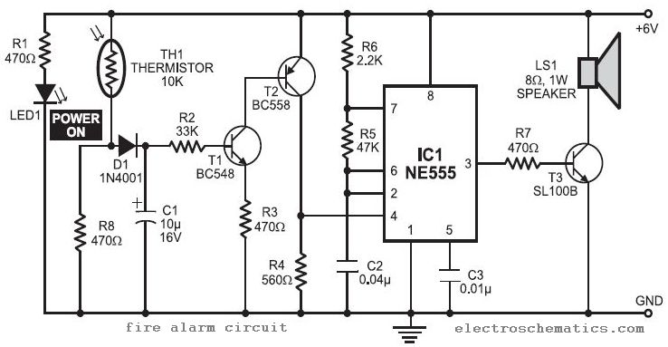
In this fire alarm circuit project, a thermistor functions as the heat sensor. When the temperature rises, its resistance decreases, and conversely, when the temperature falls, its resistance increases. Under normal conditions... In this fire alarm circuit, the thermistor is...

UPDATED 2014 This project presents the original high-power mobile phone jammer circuit, with all updates posted here. Caution is advised regarding the use of this device, as it is illegal. The purpose of sharing this circuit is solely for...
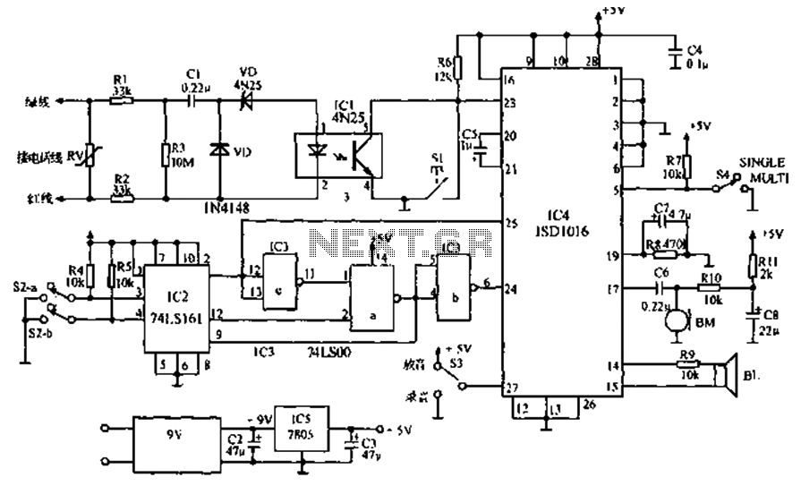
The call is made using the ISD1016 language chip for voice generation instead of a traditional phone ringing message controller schematic circuit. This controller can store messages, music, songs, or other sounds, serving as an alternative to monotonous ringing. The...
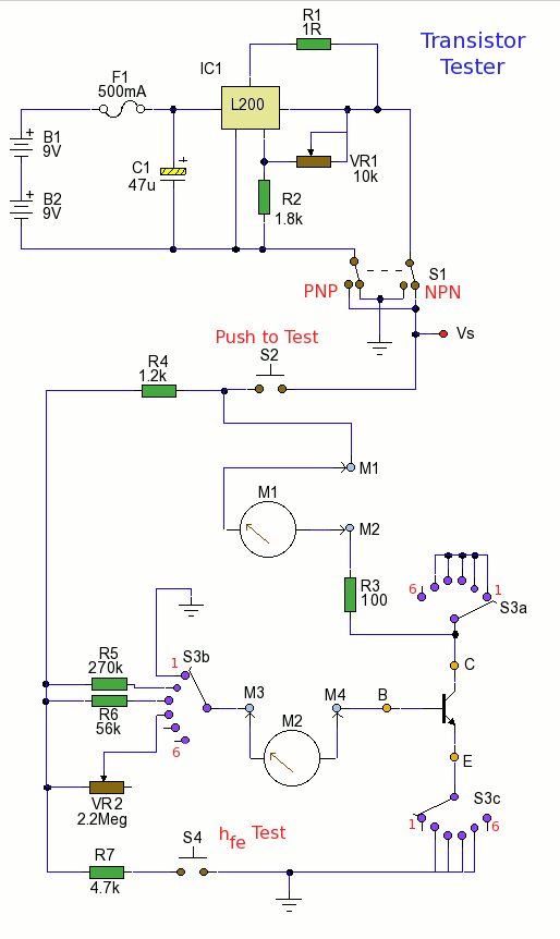
Using the tester is straightforward. Begin with the power off and insert a transistor into the test socket. Set switch S1 for either NPN or PNP configuration and rotate switch S3 to the desired test position. Adjust variable resistor...